Samsung Foundry’s 3nm and 4nm Yields Are Enhancing
At the moment, solely two foundries supply their clients 3 nm and 4 nm-class course of applied sciences: TSMC and Samsung Foundry. However enterprise media typically blames Samsung Foundry for mediocre yields on modern nodes, which can’t be verified. However a latest report issued by an funding banking agency claims that yields of Samsung’s 3 nm and 4 nm-class nodes are on fairly respectable ranges. However there’s a catch.
Samsung Foundry’s 4 nm-class course of expertise yield is now increased than 75%. In distinction, yields of chips on SF3E (3nm-class, gate-all-around early) now exceeds 60%, in keeping with estimates in a report from Hello Funding & Securities, a member of DGB Monetary Group, studies Kmib.co.kr. The identical report claims that TSMC’s yields at its N4 node method 80%, however once more, that is an estimate by a researcher.
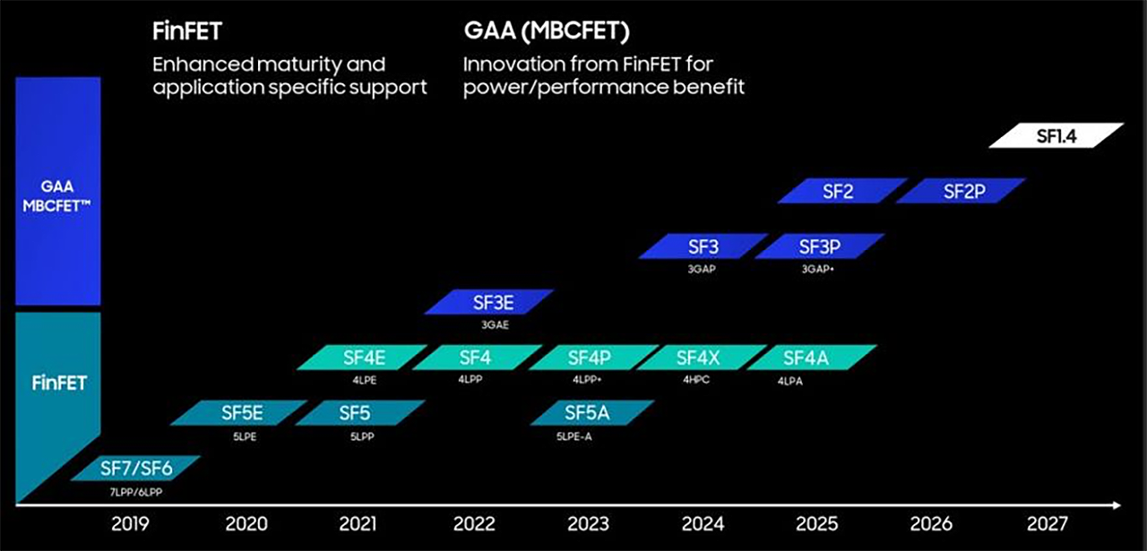
Generally, details about yields at foundries can’t be verified since contract makers of chips by no means speak about yields publicly since they rely upon a number of issues, corresponding to die measurement, efficiency targets, and design peculiarities. They generally disclose defect density publicly in comparison with earlier nodes, however that is hardly the case for Samsung Foundry’s SF4E, SF4, SF4P, and SF3E.
Formally, Samsung Foundry solely says that its SF3E course of expertise is in high-volume manufacturing with secure yields (presumably to deal with a media report from late final 12 months which stated that SF’s yields on SF3E had been unstable), and the event of refined SF3 is ongoing.
“We’re mass producing the first gen 3nm course of with secure yields, and, primarily based on this expertise, we’re growing the 2nd gen course of to safe even better mass manufacturing capabilities,” a statement by Samsung reads.
In the meantime, TechInsights found one of many first chips made on Samsung’s SF3E course of. That is the Whatsminer M56S++ which is outwardly a cryptocurrency mining chip from MicroBT, a Chinese language developer. Mining chips are tiny simplistic gadgets with a great deal of common buildings and few SRAM bit cells. Such chips are simple to make and serve completely as pipe cleaners for the most recent course of applied sciences, so it’s not stunning that Samsung Foundry is making them fairly than massive ASICs on its SF3E. In the meantime, yields of small chips are, by definition, increased than yields of enormous ASICs made on the identical node. Subsequently, if yields of the Whatsminer M56S++ are at 75% or increased, it doesn’t imply that a big smartphone or PC SoC yields shall be on the identical stage with the identical defect density.
There’s an oblique affirmation that yields of Samsung’s 5 nm and seven nm-class fabrication processes are enhancing. The utilization fee of Samsung Foundry’s for five nm-capable strains elevated to 80%, and the mixed utilization fee of 5nm and seven nm-capable fabs climbed to 90% not too long ago, up from 60% in 2022, in keeping with a DigiTimes story that cites ET Information. Once more, the knowledge comes from an unofficial supply.
Usually, fabless chip designers will not be inclined to make use of nodes with excessive defect densities, so if the utilization fee of 5 nm-class (Samsung’s SF4 derived from SF5) will get increased, this may increasingly point out that they’re now extra intensively utilized by Samsung’s clients. Alternatively, this can be an indication that Samsung Foundry has clients determined sufficient to extend manufacturing regardless of low yields as a consequence of excessive demand. But, given the present market situations, this might not be the case.
Sources: Kmib.co.kr, DigiTimes, TechInsights