CoW-SoW Stacks Up the Chips

TSMC has been providing its System-on-Wafer integration know-how, InFO-SoW, since 2020. For now, solely Cerebras and Tesla have developed wafer scale processor designs utilizing it, as whereas they’ve unbelievable efficiency and energy effectivity, wafer-scale processors are extraordinarily complicated to develop and produce. However TSMC believes that not solely will wafer-scale designs ramp up in utilization, however that megatrends like AI and HPC will name for much more complicated options: vertically stacked system-on-wafer designs.
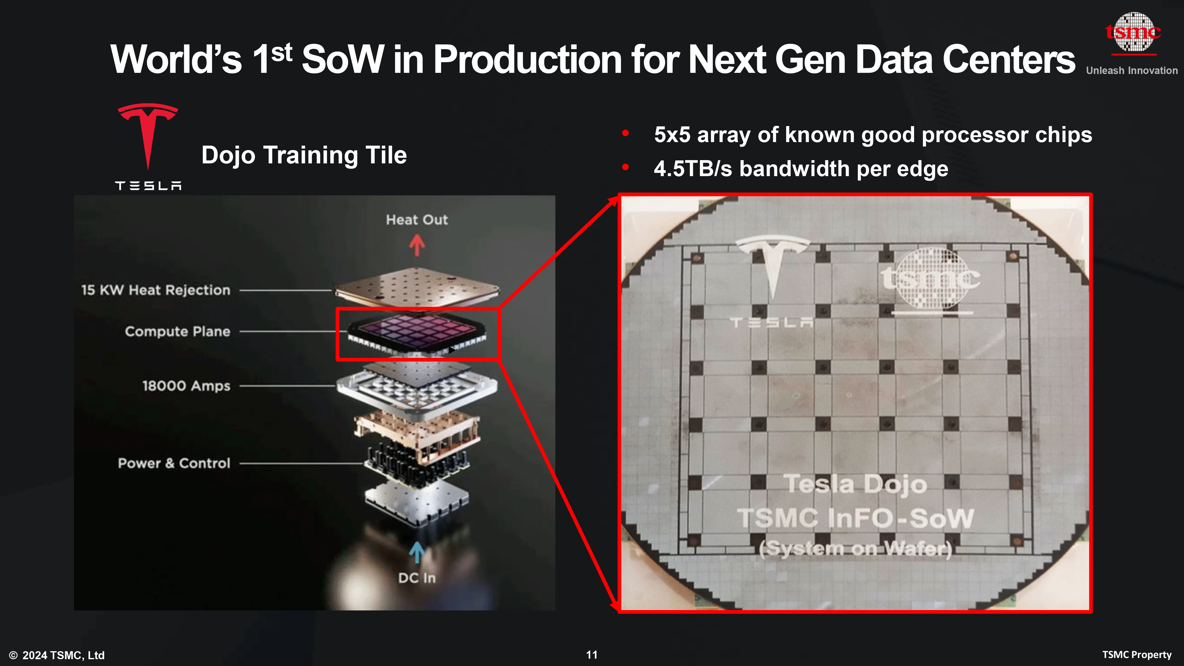
Tesla Dojo’s wafer-scale processors — the primary options primarily based primarily based on TSMC’s InFO-SoW know-how which might be in mass manufacturing — have an a variety of benefits over typical system-in-packages (SiPs), together with low-latency high-bandwidth core-to-core communications, very excessive efficiency and bandwidth density, comparatively low energy supply community impendance, excessive efficiency effectivity, and redunancy.
However with InFO-SoW and different wafer scale integration strategies, processor designers need to rely solely on on-chip reminiscence. That is completely ample for a lot of functions, but it surely might not be sufficient for next-generation AI workloads. Moreover, with InFO-SoW, the entire wafer must be processed utilizing one fabrication know-how, which might not be optimum, or too costly for sure designs.
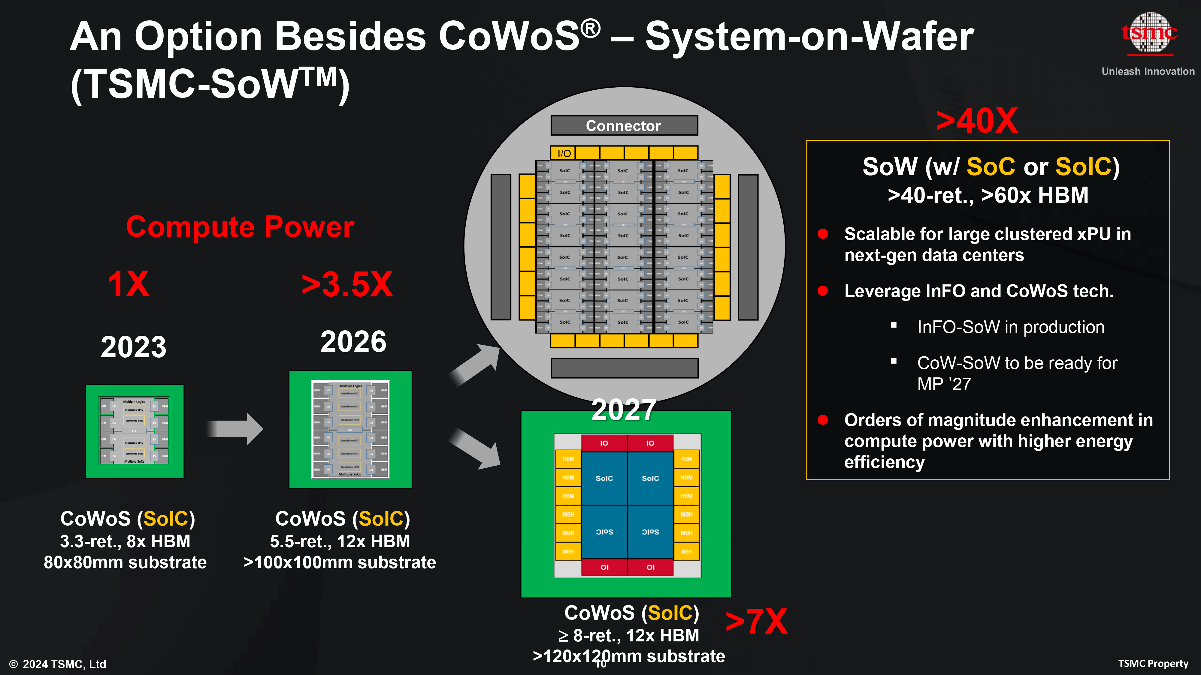
So, with its next-generation system-on-wafer platform, TSMC plans to convey collectively two of its packaging applied sciences: InFO-SoW and System on Built-in Chips (SoIC), which is able to permit it to stack reminiscence or logic on prime of a system-on-wafer utilizing its Chip-on-Wafer (CoW) technique. The CoW-SoW know-how, which the corporate introduced at its North American Know-how Symposium, shall be prepared for mass manufacturing in 2027.
For now, TSMC is generally speaking about marriage ceremony wafer scale processors with HBM4 reminiscence. And provided that HBM4 stacks will function a 2048-bit interface, its tighter integration with logic is one thing that the trade is contemplating.
“So, sooner or later, utilizing wafer degree integrations [will allow] our clients to combine much more logic and reminiscence collectively,” mentioned Kevin Zhang, Vice President of Enterprise Improvement at TSMC. “SoW is now not a fiction, that is one thing we already work with our clients [on] to provide a few of the merchandise already in place. This we predict by leveraging our superior wafer degree integration know-how, we are able to present our buyer an important the trail permit them to proceed to develop their functionality to herald extra computation, extra vitality environment friendly computation, to their AI cluster or [supercomputer].”