TSMC Preps Cheaper 4nm N4C Course of For 2025, Aiming For 8.5% Price Discount

Whereas the majority of consideration on TSMC is geared toward its modern nodes, akin to N3E and N2, a great deal of chips will proceed to be made utilizing extra mature and confirmed course of applied sciences for years to come back. Which is why TSMC has continued to refine its current nodes, together with its current-generation 5nm-class choices. To that finish, at its North American Expertise Symposium 2024, the corporate launched a brand new, optimized 5nm-class node: N4C.
TSMC’s N4C course of belongs to the corporate’s 5nm-class household of fab nodes and is a superset of N4P, essentially the most superior expertise in that household. In a bid to additional convey down 5nm manufacturing prices, for TSMC is implementing a number of modifications for N4C, together with rearchitecting their normal cell and SRAM cell, altering some design guidelines, and decreasing the variety of masking layers. Because of these enhancements, the corporate expects N4C to attain each smaller die sizes in addition to a discount in manufacturing complexity, which in flip will convey die prices down by as much as 8.5%. Moreover, with the identical wafer-level defect density charge as N4P, N4C stands to supply even greater useful yields because of its die space discount.
“So, we’re not completed with our 5nm and 4nm [technologies],” stated Kevin Zhang, Vice President of Enterprise Growth at TSMC. “From N5 to N4, now we have achieved 4% density enchancment optical shrink, and we proceed to boost the transistor efficiency. Now we usher in N4C to our 4 nm expertise portfolio. N4C permits our clients to cut back their prices by take away a few of the masks and to additionally enhance on the unique IP design like a normal cell and SRAM to additional cut back the general product stage value of possession.”
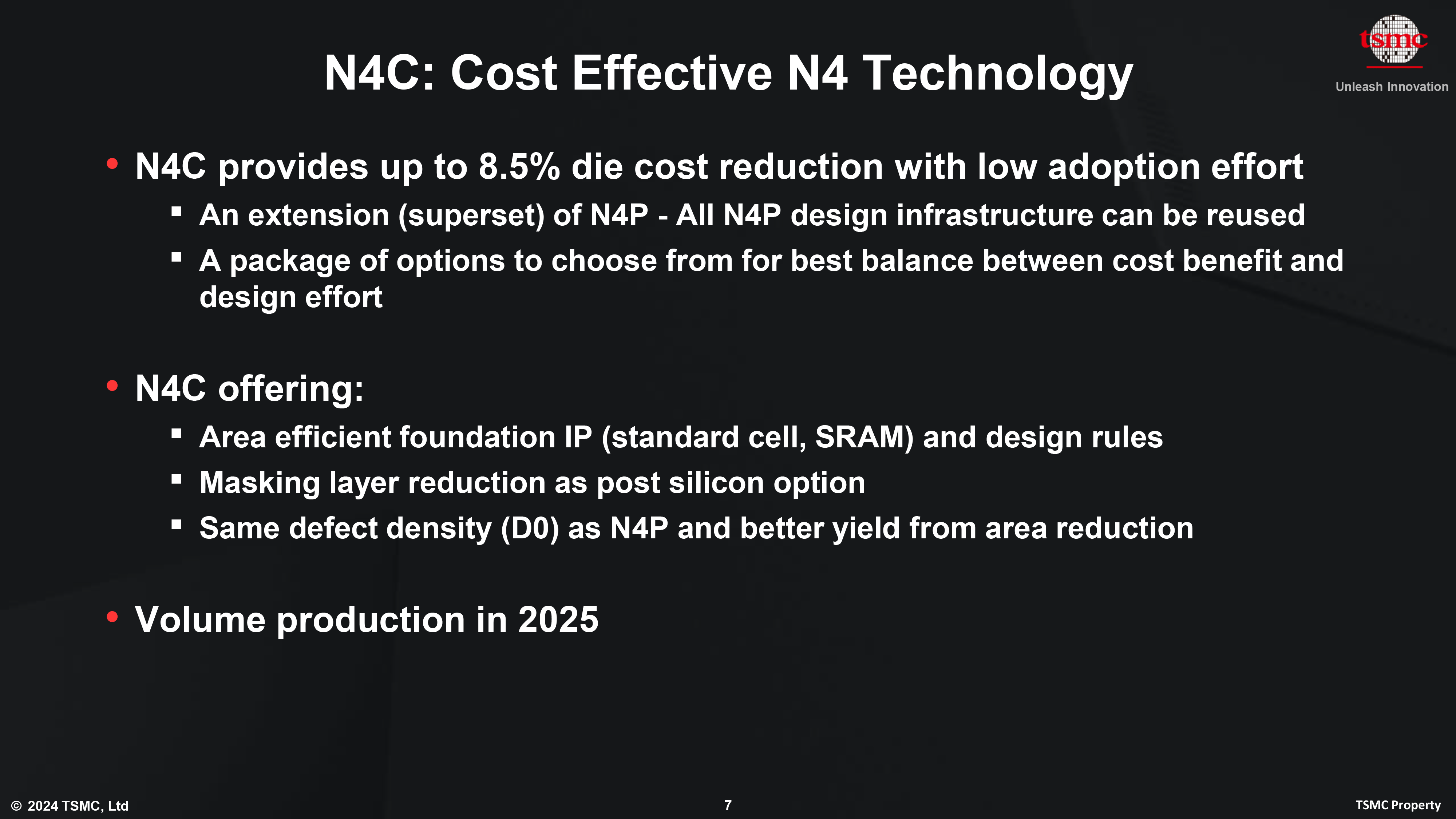
TSMC says that N4C can use the identical design infrastructure as N4P, although it’s unclear whether or not N5 and N4P IP will be re-used for N4C-based chips. In the meantime, TSMC signifies that it presents numerous choices for chipmakers to seek out the best steadiness between value advantages and design effort, so firms excited by adopting a 4nm-class course of applied sciences might effectively undertake N4C.
The event of N4C comes as a lot of TSMC’s chip design clients are getting ready to launch chips primarily based on the corporate’s remaining era of FinFET course of expertise, the 3nm N3 collection. Whereas N3 is predicted to be a profitable household, the excessive prices of N3B have been a problem, and the era is marked by diminishing efficiency and transistor density returns altogether. Consequently, N4C might effectively turn out to be a serious, long-lived node at TSMC, serving as an excellent match for patrons who wish to follow a more cost effective FinFET node.
“This can be a very important enhancement, we’re working with our buyer, mainly to extract extra worth from their 4 nm funding,” Zhang stated.
TSMC expects to begin quantity manufacturing of N4C chips a while subsequent 12 months. And with TSMC having produced 5nm-class for practically half a decade at that time, N4C ought to be capable of hit the bottom operating by way of quantity and yields.