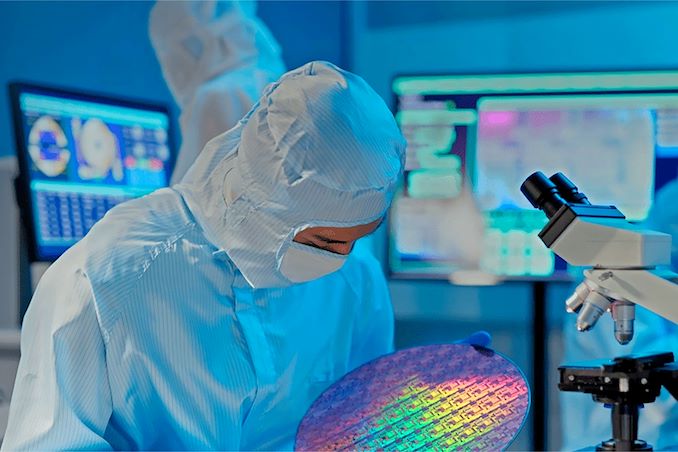
Samsung’s Subsequent-Gen 3nm and 4nm Nodes on Observe for Mass Manufacturing in 2H 2024
Samsung is about to start out making chips utilizing its 2nd Technology 3nm-class (SF3) manufacturing expertise in addition to performance-enhanced model of its 4nm-class (SF4X) fabrication course of within the second half of subsequent 12 months, the corporate informed its traders this week. Each manufacturing nodes are anticipated to considerably enhance aggressive positions of the corporate as they are going to allow it to construct new kinds of merchandise.
“We are going to strengthen our expertise competitiveness via the 2H [2024] mass manufacturing of the 2nd technology 3nm course of in addition to the 4th technology 4nm course of for HPC,” an announcement by the corporate reads. “The market is forecast to shift to development due to a rebound in cellular demand and continued development in HPC demand.”
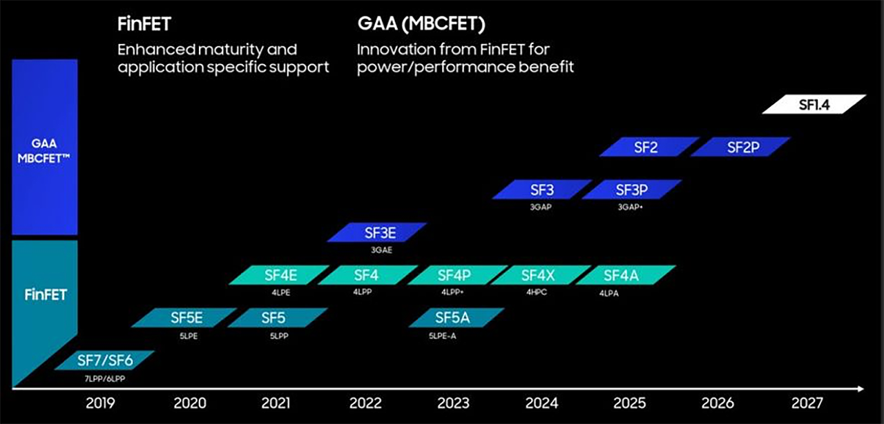
Samsung’s forthcoming SF3 course of expertise is a main improve to its present SF3E manufacturing node, which, based mostly on the obtainable data, is just used to make small chips for cryptocurrency mining. Samsung asserts that the SF3 will provide larger design versatility by permitting for various gate-all-around (GAA) transistor’s nanosheet channel widths inside the identical cell sort.
Though Samsung doesn’t make direct comparisons between SF3 and SF3E, it says that SF3 gives main enhancements over SF4 (4LPP, 4nm-class, low energy plus), which incorporates a 22% improve in efficiency at equal energy and complexity, or alternatively, a 34% discount in energy consumption on the identical frequency and transistor rely, together with a 21% discount in logic space. Usually, it’s anticipated that SF3 can be a greater possibility for complicated designs than SF3E, although it’ll enter high-volume manufacturing within the second half of 2024.
Within the meantime, Samsung Foundry’s 4nm-class technology nodes proceed to evolve. The corporate gearing as much as launch its SF4X (4HPC, 4 nm-class high-performance computing) course of expertise, tailor-made for high-performance functions reminiscent of CPUs and GPUs utilized in information facilities. This one goes to be SF’s first course of node in current years that has been particularly designed for high-performance computing (HPC) functions.
Samsung’s SF4X course of expertise guarantees to ship a ten% enchancment in efficiency together with a 23% discount in energy consumption. Whereas Samsung has not disclosed the baseline for this comparability, it’s possible in reference to their normal SF4 (4LPP) course of. This enhancement is achieved via a redesign of the transistor’s supply and drain areas, following a reassessment of their efficiency beneath doubtlessly high-stress situations, the applying of superior transistor-level design-technology co-optimization (T-DTCO), and the implementation of a new middle-of-line (MOL) structure.
With refined MOL structure, SF4X is predicted to realize a silicon-validated minimal working voltage (Vmin) for CPUs at 60mV, scale back the variability within the off-state present (IDDQ) by 10%, guarantee steady excessive voltage (Vdd) operation above 1V with out compromising efficiency, and improve course of margin for SRAM.