HBM Hits 36GB Stacks at 9.8 Gbps
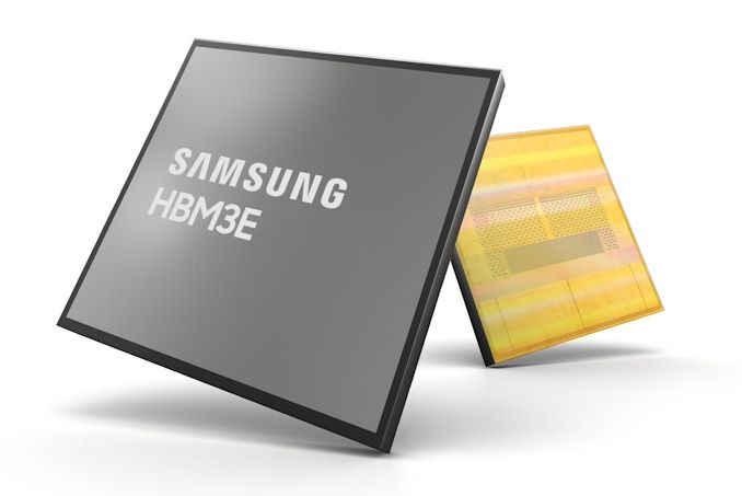
Samsung’s annual Reminiscence Tech Day is happening in San Jose this morning, and as a part of the occasion, the corporate is making a few notable reminiscence expertise bulletins/disclosures. The spotlight of Samsung’s occasion is the introduction of Shinebolt, Samsung’s HBM3E reminiscence that may set new marks for each reminiscence bandwidth and reminiscence capability for high-end processors. The corporate can be disclosing a bit extra on their GDDR7 reminiscence, which is able to mark a big technological replace to the GDDR household of reminiscence requirements.
Beginning issues off, we have now as we speak’s marquee announcement: Shinebolt HBM3E reminiscence. Like the remainder of the reminiscence trade, Samsung is making ready a successor to the current-generation of HBM3 reminiscence that’s getting used with high-end/HPC-grade processors, with the trade settling across the upcoming HBM3E standard. HBM3E is slated to supply each considerably increased capacities and higher reminiscence bandwidth than HBM3, serving to the high-bandwidth reminiscence expertise sustain with ever-growing workloads on high-end processors.
| Samsung HBM Reminiscence Generations | ||||||
| HBM3E (Shinebolt) |
HBM3 (Icebolt) |
HBM2E (Flashbolt) |
HBM2 (Aquabolt) |
|||
| Max Capability | 36GB | 24 GB | 16 GB | 8 GB | ||
| Max Bandwidth Per Pin | 9.8 Gb/s | 6.4 Gb/s | 3.6 Gb/s | 2.0 Gb/s | ||
| Variety of DRAM ICs per Stack | 12 | 12 | 8 | 8 | ||
| Efficient Bus Width | 1024-bit | |||||
| Voltage | ? | 1.1 V | 1.2 V | 1.2 V | ||
| Bandwidth per Stack | 1.225 TB/s | 819.2 GB/s | 460.8 GB/s | 256 GB/s | ||
The premise of Shinebolt is a brand new 24Gbit HBM reminiscence die, which Samsung might be producing on their D1a course of, the corporate’s EUV-based 4th era 10nm-class (14nm) node. Samsung might be producing each 8Hi and ultimately 12Hi stacks based mostly on this new die, permitting for whole stack capacities of 24GB and 36GB respectively, 50% extra capability than their HBM3 (Icebolt) equivalents.
In response to Samsung, Shinebolt will be capable of hit reminiscence clockspeeds as excessive as 9.8Gbps/pin, higher than 50% sooner than their HBM3 merchandise. Although given a few of Samsung’s earlier reminiscence clockspeed claims, there’s an excellent likelihood this can be a semi-overclocked state. Shinebolt improvement isn’t far sufficient alongside for Samsung to checklist particular person SKUs, however even on the conservative finish of issues, Samsung is selling information charges of not less than 8Gbps/pin of their occasion press launch. And if Samsung’s formidable reminiscence frequencies do come to fruition, then that will put Samsung forward of their competitors as effectively; so far, SK hynix and Micron have introduced plans for 9Gbps/pin and 9.2Gbps/pin reminiscence respectively, so Samsung’s claims are actually essentially the most aggressive.
General, these clockspeeds would give a single HBM3E stack a minimal bandwidth of 1TB/sec, and a most bandwidth of 1.225TB/sec, effectively forward of the 819GB/sec information price of HBM3. Or to border issues in reference of a high-end processor (e.g. NVIDIA H100), a 6-stack chip would be capable of entry as a lot as 216GB of reminiscence with an combination reminiscence bandwidth as excessive as 7.35TB/sec.
As for energy effectivity, issues look to be a little bit of a combined bag. On a relative foundation, Samsung says that Shinebolt might be 10% extra environment friendly than Icebolt – in different phrases, consuming 10% much less energy per bit transferred (pJ/bit). Nevertheless, a 25%+ clockspeed enchancment will greater than wipe out these positive factors as a result of vital improve in bits transferred. So whereas Shinebolt might be extra environment friendly general, on an absolute foundation plainly whole energy consumption for HBM reminiscence will proceed to develop with the subsequent era.
Both manner, for the high-end processor market that Samsung is focusing on with Shinebolt, chipmakers are unlikely to be fazed by the ability improve. Like the remainder of the high-end processor house, Samsung has the AI market set sq. in its sights – a market phase the place each reminiscence bandwidth and reminiscence capability are limiting components, particularly with large massive language fashions (LLMs). Together with the normal supercomputer and networking market segments, Samsung ought to have little bother promoting sooner HBM in the midst of a booming AI market.
Like the opposite main reminiscence distributors, Samsung expects to ship Shinebolt sooner or later in 2024. On condition that the corporate simply began sampling the reminiscence – and that HBM3 Icebolt itself simply hit mass manufacturing – Shinebolt’s probably not delivery till the later a part of the yr.
A Transient Teaser on HBM4: FinFETs & Copper-to-Copper Bonding
Lastly, trying even farther into the long run, Samsung is briefly speaking about their plans for HBM4 reminiscence. Whereas that expertise remains to be a couple of years off (there’s not even an accredited specification for it but), we all know from previous disclosures that the reminiscence trade is aiming to maneuver to a wider, 2048-bit reminiscence interface. Which, as Samsung likes to border issues, is the one sensible alternative when additional HBM clockspeed will increase would blow out energy consumption.
For HBM4, Samsung is taking a look at using extra superior fab and packaging applied sciences which can be presently the area of logic chips. On the fab aspect of issues, the corporate desires to maneuver to utilizing FinFET transistors for his or her reminiscence, versus the planar transistors nonetheless used there. As with logic, FinFETs would cut back the drive present required, which might assist to enhance DRAM power effectivity. In the meantime on the packaging aspect of issues, Samsung is taking a look at shifting from micro-bump bonding to bumpless (direct copper-to-copper) bonding, a packing approach that’s nonetheless on the cutting-edge of improvement even within the logic house. Embracing cutting-edge applied sciences might be vital to holding HBM bandwidth rising because it has over the past decade, however the prices and complexities of doing so additionally underscore why HBM stays an solely area of interest high-end reminiscence expertise.
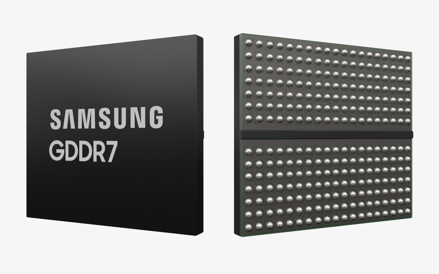
GDDR7 Replace: 50% Decrease Stand-By Energy Than GDDR6
Moreover HBM3E, Samsung’s different large bandwidth reminiscence replace of the day is a quick standing replace on their GDDR7 reminiscence.
Again in July of this yr, Samsung announced that they completed initial development on their GDDR7 memory. The following era of GDDR reminiscence, GDDR7 brings with it a number of main modifications versus as we speak’s GDDR6, essentially the most vital of which is a swap to PAM3 encoding. PAM3 permits for 1.5 bits to be transferred per cycle (or quite 3 bits over two cycles), opening the door to bettering reminiscence switch charges with out using extra pricey technique of additional bettering the frequency of the reminiscence bus.
| GDDR Reminiscence Generations | |||||
| GDDR7 | GDDR6X | GDDR6 | |||
| B/W Per Pin | 32 Gbps (Projected) | 24 Gbps (Transport) | 24 Gbps (Sampling) | ||
| Chip Density | 2 GB (16 Gb) | 2 GB (16 Gb) | 2 GB (16 Gb) | ||
| Whole B/W (256-bit bus) | 1024 GB/sec | 768 GB/ssec | 768 GB/ssec | ||
| DRAM Voltage | 1.2 V | 1.35 V | 1.35 V | ||
| Knowledge Charge | QDR | QDR | QDR | ||
| Signaling | PAM-3 | PAM-4 | NRZ (Binary) | ||
| Packaging | 266 FBGA | 180 FBGA | 180 FBGA | ||
As a fast recap from Samsung’s July announcement, Samsung might be rolling out 16Gbit (2GB) modules, which is able to be capable of run at as much as 32Gbps/pin. That’s a 33% enchancment in bandwidth per pin over present GDDR6 reminiscence, and would carry the combination bandwidth of a 256-bit reminiscence bus to a cool 1TB/second. GDDR7 also needs to ship a 20% enchancment in energy effectivity over Samsung’s GDDR6 (when it comes to pJ/bit), thanks partially to the usage of Samsung’s 3rd era D1z (10nm-class) fab node.
At present’s occasion from Samsung is essentially a recap of July’s announcement, however within the course of we have now realized a few new technical particulars on GDDR7 that Samsung hasn’t beforehand disclosed. First off, GDDR7 isn’t simply bettering energetic energy consumption, however the tech can even enhance on stand-by energy consumption to a big diploma. Due to extra clock controls, GDDR7 will eat 50% much less stand-by energy than GDDR6.
Second, in discussing why Samsung (and the trade as a complete) went with PAM3 encoding for GDDR7 as an alternative of even denser PAM4, the corporate confirmed a few of our technical suppositions on the brand new expertise. In brief, PAM3 has a decrease common bit error price (BER) than PAM4, largely because of the broader margins on the attention window. None of which makes PAM4 unworkable (as Micron has already confirmed), however Samsung and the remainder of the reminiscence trade are favoring the relative simplicity of PAM3, given the trade-offs.
Moreover the standard video card/gaming prospects, Samsung is anticipating GDDR7 to be adopted by AI chip makers, and maybe a bit extra surprisingly, the automotive trade. In actual fact a few of these non-traditional prospects could be the first to undertake the reminiscence; for the reason that conventional GPU distributors are nonetheless mid-cycle on their present era of merchandise, it should nonetheless be fairly a while earlier than they ship any GDDR7-capable silicon.
At this level Samsung has not introduced a projected date for when their GDDR7 reminiscence will go into mass manufacturing. However the firm remains to be anticipating that they would be the first vendor to ship the next-generation reminiscence, presumably in 2024.