HBM4 in Growth, Organizers Eyeing Even Wider 2048-Bit Interface
Excessive-bandwidth reminiscence has been round for a few decade, and all through its its continued improvement it has steadily elevated in velocity, beginning at a knowledge switch price from 1 GT/s (the unique HBM) and reaching upwards of 9 GT/s with the forthcoming HBM3E. This has made for a powerful soar in bandwidth in lower than 10 years, making HBM an necessary cornerstone for complete new lessons of HPC accelerators which have since hit the market. Nevertheless it’s additionally a tempo that is getting more durable to maintain as reminiscence switch charges enhance, particularly because the underlying physics of DRAM cells haven’t modified. In consequence, for HBM4 the main reminiscence producers behind the spec are planning on making a extra substantial change to the high-bandwidth reminiscence know-how, beginning with an excellent wider 2048-bit reminiscence interface.
Designed as a wide-but-slow reminiscence know-how that makes use of an ultra-wide interface working at a comparatively modest clockspeed, HBM’s present 1024-bit reminiscence interface has been a defining attribute of the know-how. In the meantime its modest clockspeeds have turn out to be more and more much less modest so as to maintain bettering reminiscence bandwidth. This has labored to this point, however as clockspeeds enhance, the extremely parallel reminiscence is risking working into the identical sign integrity and vitality effectivity points that problem GDDR and different extremely serial reminiscence applied sciences.
Consequently, for the following era of the know-how, organizers are going wider as soon as extra, increasing the width of the HBM reminiscence interface even additional to 2048-bits. And, equally as necessary for a number of technical causes, they intend to do that with out growing the footprint of HBM reminiscence stacks, primarily doubling the interconnection density for the next-generation HBM reminiscence. The online consequence could be a reminiscence know-how with an excellent wider reminiscence bus than HBM at the moment, giving reminiscence and gadget distributors room to additional enhance bandwidth with out additional growing clock speeds.
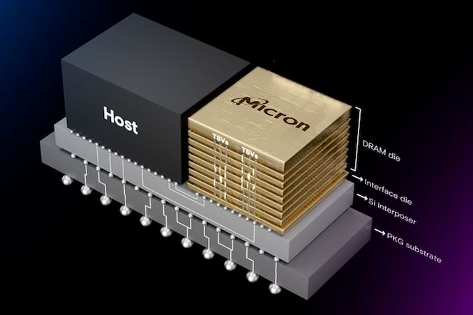
As deliberate, this is able to make HBM4 a serious technical leap ahead on a number of ranges. On the DRAM stacking facet of issues, a 2048-bit reminiscence interface goes to require a major enhance within the variety of through-silicon vias routed by way of a reminiscence stack. In the meantime the exterior chip interface would require shrinking the bump pitch to effectively under 55 um, all of the whereas growing the whole variety of micro bumps considerably from the present depend of (round) 3982 bumps for HBM3.
Including some extra complexity to the know-how, reminiscence makers have indicated that also they are going to stack as much as 16 reminiscence dies in a single module; so-called 16-Hello stacking. (HBM3 technically supports 16-Hello stacks as effectively, however up to now no producer is definitely utilizing it) This can permit reminiscence distributors to considerably enhance the capability of their HBM stacks, nevertheless it brings new complexity in wiring up an excellent bigger variety of DRAM dies with out defects, after which protecting the ensuing HBM stack suitably and persistently brief.
All of this, in flip would require even nearer collaboration between chip makers, reminiscence makers, and chip packaging companies so as to make the whole lot come collectively easily.
Talking at TSMC’s OIP 2023 convention in Amsterdam, Dan Kochpatcharin, TSMC’s Head of Design Infrastructure Administration had this to say: “As a result of as a substitute of doubling the velocity, they doubled the [interface] pins [with HBM4]. That’s the reason we’re pushing to be sure that we work with all three companions to qualify their HBM4 [with our advanced packaging methods] and in addition be sure that both RDL or interposer or no matter in between can assist the structure and the velocity [of HBM4]. So, [we work with] Samsung, SK Hynix, and Micron.”
Since system-in-package (SiP) designs are getting bigger, and the variety of HBM stacks supported by superior chip packages is growing (e.g. 6x reticle size interposers and chips with 12 HBM stacks on-package), chip packages are getting extra complicated. To make sure that the whole lot continues to work collectively, TSMC is pushing chip and reminiscence designers to embrace Design Know-how Co-Optimization (DTCO). This being an enormous a part of the rationale why the world’s largest foundry not too long ago organized 3DFabric Reminiscence Alliance, a program designed to allow shut collaboration between DRAM makers and TSMC in a bid to allow next-generation options that can pack big quantities of logic transistors and superior reminiscence.
Amongst different issues, TSMC’s 3DFabric Reminiscence Alliance is at the moment engaged on guaranteeing that HBM3E/HBM3 Gen2 reminiscence works with CoWoS packaging, 12-Hello HBM3/HBM3E packages are suitable with superior packages, UCIe for HBM PHY, and buffer-less HBM (a know-how spearheaded by Samsung).
General, TSMC’s feedback final week give us our greatest look but on the subsequent era of high-bandwidth reminiscence. Nonetheless, extra technical particulars about HBM4 stay slightly scarce for the second. Micron said earlier this year that ‘HBMNext’ reminiscence set to reach round 2026 will supply capacities between 36 GB and 64 GB per stack and peak bandwidth of two TB/s per stack or greater. All of which signifies that reminiscence makers will not be backing off on reminiscence interface clockspeeds for HBM4, even with the transfer to a wider reminiscence bus.