Intel Exhibits Off Work on Subsequent-Gen Glass Core Substrates, Plans Deployment Later in Decade

Though Intel’s annual Innovation occasion doesn’t kick off till tomorrow, the corporate is already publishing some bulletins forward of the present – and it’s not the trivial stuff, both. This morning the corporate is exhibiting off their preliminary work on creating a glass core substrate and related packaging course of for his or her chips. On account of their progress with analysis and improvement on the glass cores, Intel is now planning on introducing glass core substrates to its merchandise within the second half of this decade, permitting them to bundle chips in additional advanced, and in the end higher-performing configurations.
There’s so much to unpack from Intel’s comparatively brief announcement, however at a excessive stage, glass core substrates have been below analysis throughout the business for over a decade as a substitute for natural substrates, that are broadly utilized in current-generation processors. Basically the medium that typical silicon dies sit on, substrates play an essential half in chip packaging. Initially, they supply the structural stability for a chip (silicon dies are fairly fragile and flimsy), and they’re additionally the means via which alerts from silicon dies are carried, both to different on-package dies (i.e. chiplets), or to the big variety of comparatively sizable pins/pads on the again facet of a chip. And, as chip sizes have elevated through the years – and the variety of pins/alerts required by high-end chips has, as effectively – so has the necessity for newer and higher supplies to make use of as a substrate, which is what’s been driving Intel’s newest accomplishment.
Finally, what Intel is aiming to do with glass core substrates is to enhance upon what might be executed with present natural substrates, permitting for bigger chips with extra alerts to be routed via the substrate extra cleanly. And whereas it will probably have advantages for all chips over an extended sufficient time, the rapid focus is on high-end, multi-chiplet processors, the place glass core substrates will provide higher mechanical stability, higher sign integrity, and the power to extra simply route a bigger variety of alerts via a non-silicon medium. In brief, Intel considers it one of many keys to creating high-performance processors within the subsequent decade.
Substrates: A Fast Recap
The necessity for substrates goes again to a number of the earliest days for large-scale built-in chips, the place chip designs reached hundreds and tens of hundreds of transistors. These small transistors wanted to be wired to a lot bigger pins as a way to be put in in methods by comparatively huge human arms, main as much as the primary chip packages, comparable to twin in-line packages. These used a body – sometimes a lead frame – to carry the precise silicon die, with the body (or alternatively, wire bonds) offering the sign paths between the die and exterior pins.
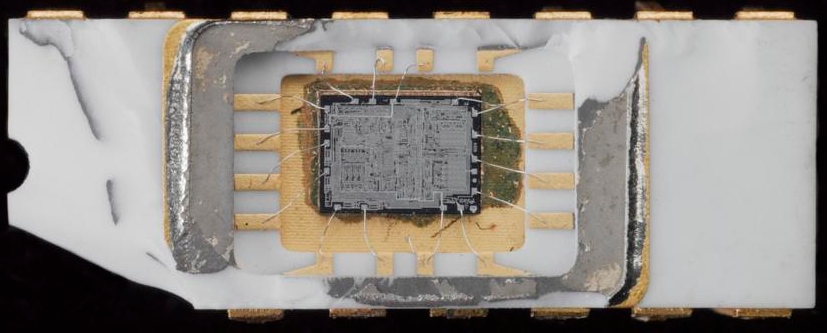
Intel 4004 Delidded (Picture Courtesy Science Museum Group Collection Online – CC BY-SA 4.0)
Because the 70s, there have been a number of evolutions in substrate designed. Metallic frames gave technique to basic ceramic chip within the 90s, after which natural packaging across the flip of the millennium. Every iteration of substrate had higher properties than the final, above all else, making it simpler to route a bigger variety of sign and energy pins to more and more advanced dies.
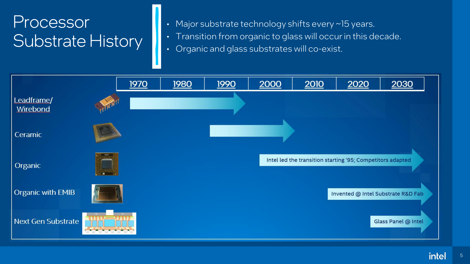
When you’ll nonetheless discover lead body and ceramic chips right here and there, natural substrates have been the bread and butter of the business for the final couple of many years. The natural materials, primarily made from PCB-like materials layered with woven glass laminates, permits for a pretty big variety of alerts to be routed via a chip, together with primary chiplet designs comparable to Intel’s cellular processors (with PCH separate PCH and CPU dies) in addition to AMD’s chiplet-based Zen processors.
However natural substrates have already been a limiting issue for a while now, particularly in high-end chips. Which is why over the past decade we’ve seen the rise of ultra-high-density interconnect interfaces comparable to silicon interposers (chip on wafer on substrate), and their derivatives like Intel’s personal EMIB. These have allowed corporations to bridge collectively the important paths of their chips with quick and dense items of silicon, however at pretty excessive prices, and with out fully resolving the drawbacks of natural substrates. Because of this, Intel has additionally been trying to find a real substitute for natural substrates, one that may play properly with massive chips, and whereas not changing the necessity for CoWoS/EMIB on the highest stage, would provide higher sign efficiency and denser routing than natural substrates right now.
Glass Core Substrates: Finer, But Stronger
This brings us to the subject of right now’s announcement from Intel, glass core substrates. The corporate has been engaged on changing natural substrates with glass for over a decade now, and so they’ve lastly reached the purpose of progress the place they’re prepared to point out it off to the world whereas planning for its use in future merchandise.
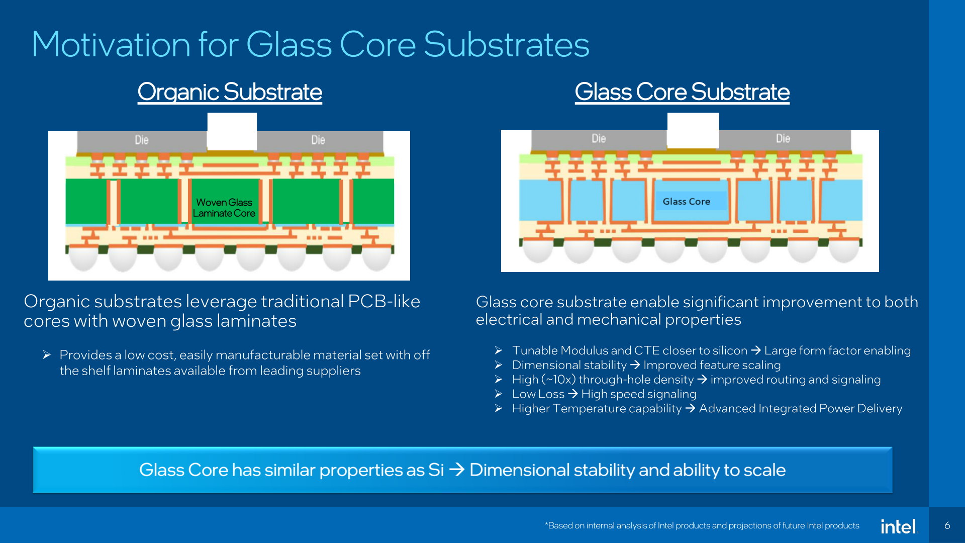
At a excessive stage, a glass core substrate is simply that: changing the natural, PCB-like materials of an natural bundle with glass. To make certain, this doesn’t imply changing the total substrate with glass – so Intel is just not going to be mounting chips on pure items of glass – however reasonably, the fabric on the core of the substrate can be made from glass. In the meantime, steel redistribution layers (RDLs) would nonetheless be current on each side of a chip, offering the precise pathways between numerous pads and solder joints.
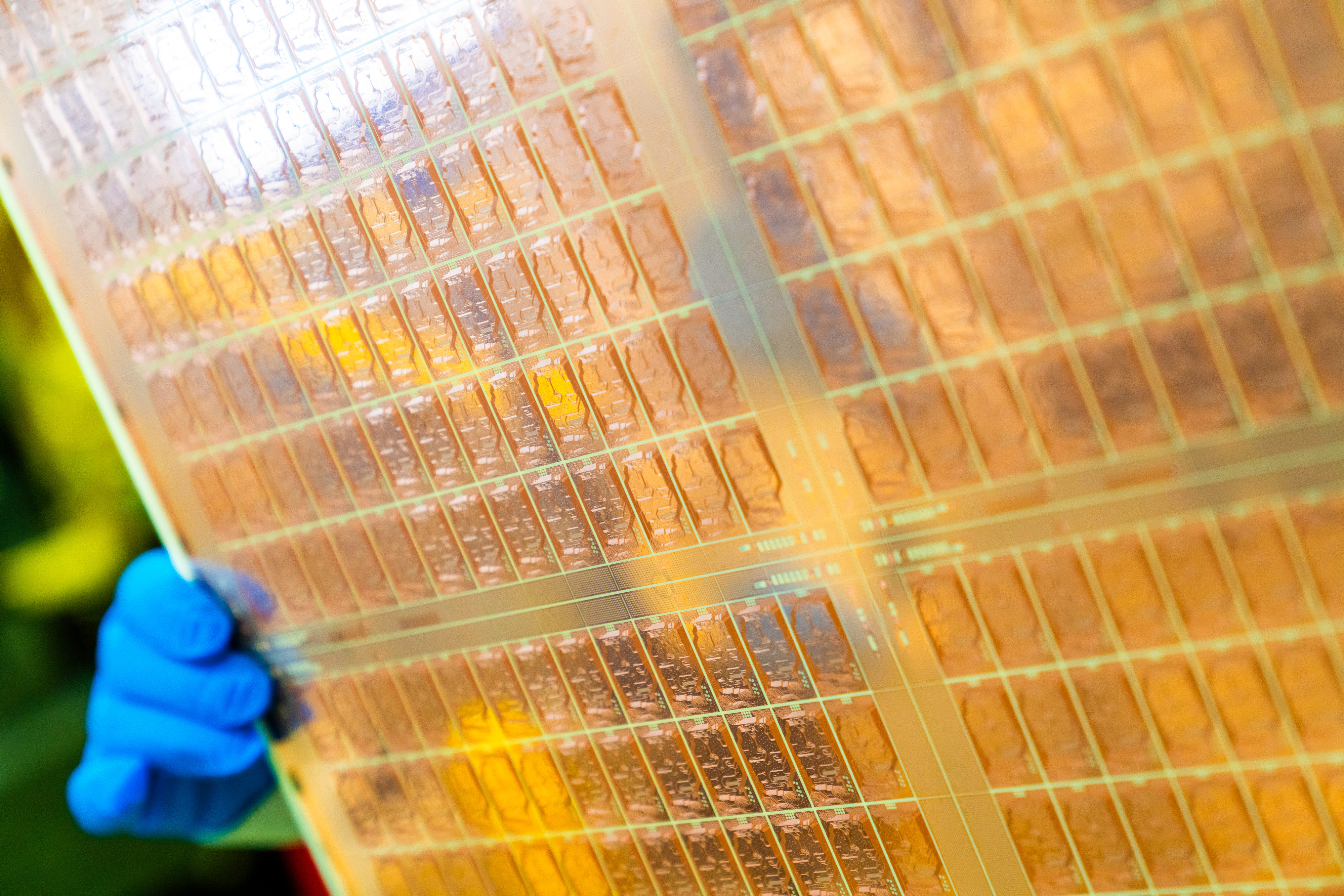
Glass Core Substrates In Panel Kind
Whereas tougher to work with than the now well-established natural substrate, Intel considers glass substrates to be superior each in mechanical and electrical properties, which in flip makes them fascinating to make use of in future chips. Or, conversely, much less undesirable than natural substrates when constructing very massive chips.
Ranging from the mechanical facet of matter, Intel reviews that cup core substrates provide much better mechanical power than natural substrates. They’re in a position to face up to greater temperatures higher than natural substrates throughout packaging, leading to much less warping and distortion. Glass can also be reportedly simpler to get flatter as effectively, which makes packaging and lithography simpler. Lastly, glass has an analogous coefficient of thermal growth as silicon (in contrast to natural substrates), that means that what little warping that also happens from warmth is in keeping with the dies above, versus having totally different elements of a chip increasing at totally different charges.
Most significantly, maybe, is that each one of these gadgets taken collectively open the door to producing bigger chips. With a extra secure substrate to mount the dies on, will probably be attainable to have bigger dies and a bigger variety of dies all sharing a single substrate – and thus behaving as a single chip.
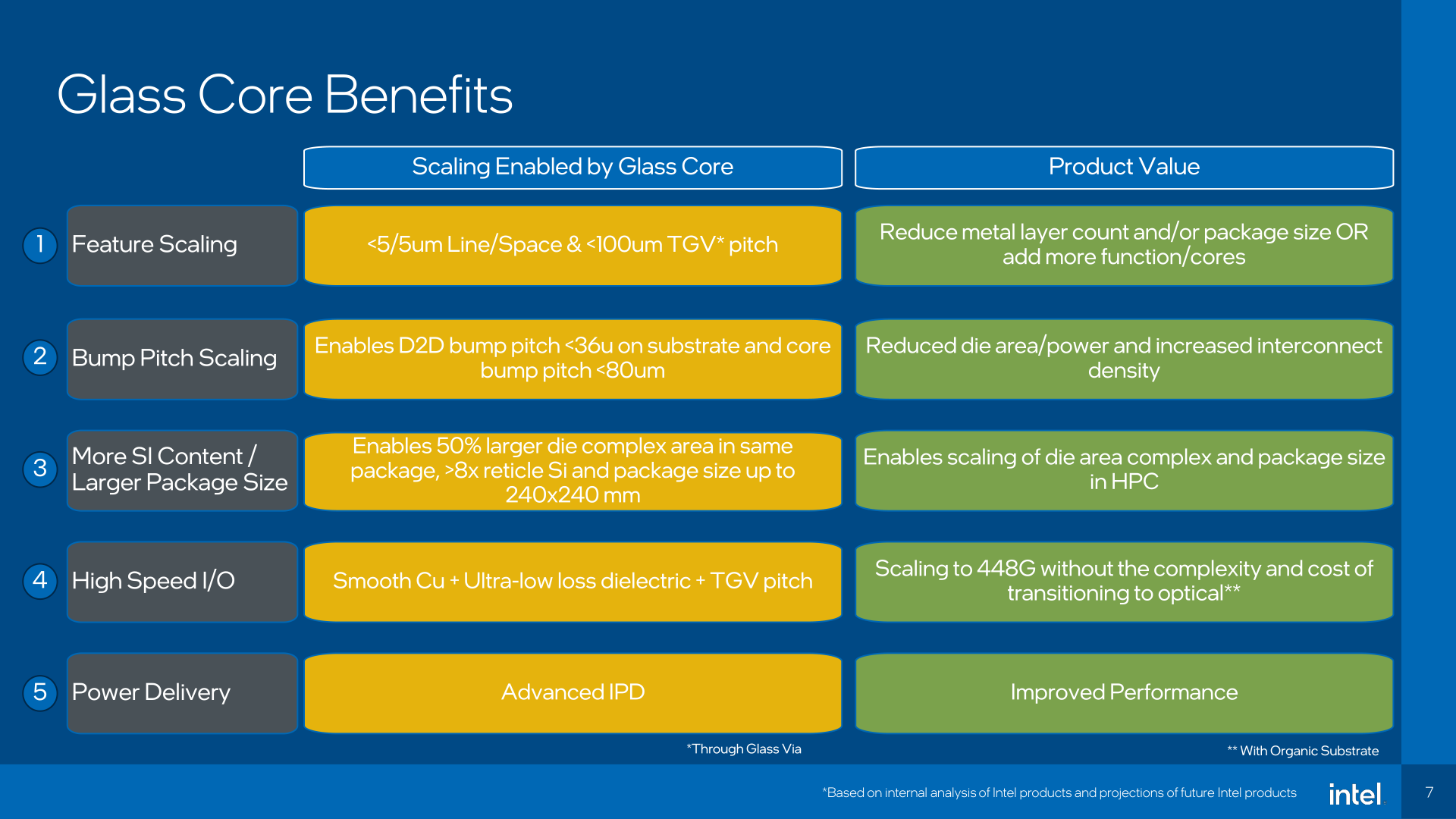
Bridging the hole between mechanical and electrical, in response to Intel, they’re additionally in a position to obtain a a lot tighter pitch on the through-glass vias (TGVs) that carry alerts via the substrate itself, permitting for a a lot bigger variety of vias general. Intel is reporting that they’re in a position to area TGVs lower than 100 microns (µm) aside, permitting for a 10-fold enchancment in TGV density. All of which in the end permits for extra flexibility in routing alerts via the substrate core, and to some extent makes it simpler to route alerts with fewer RDL layers.
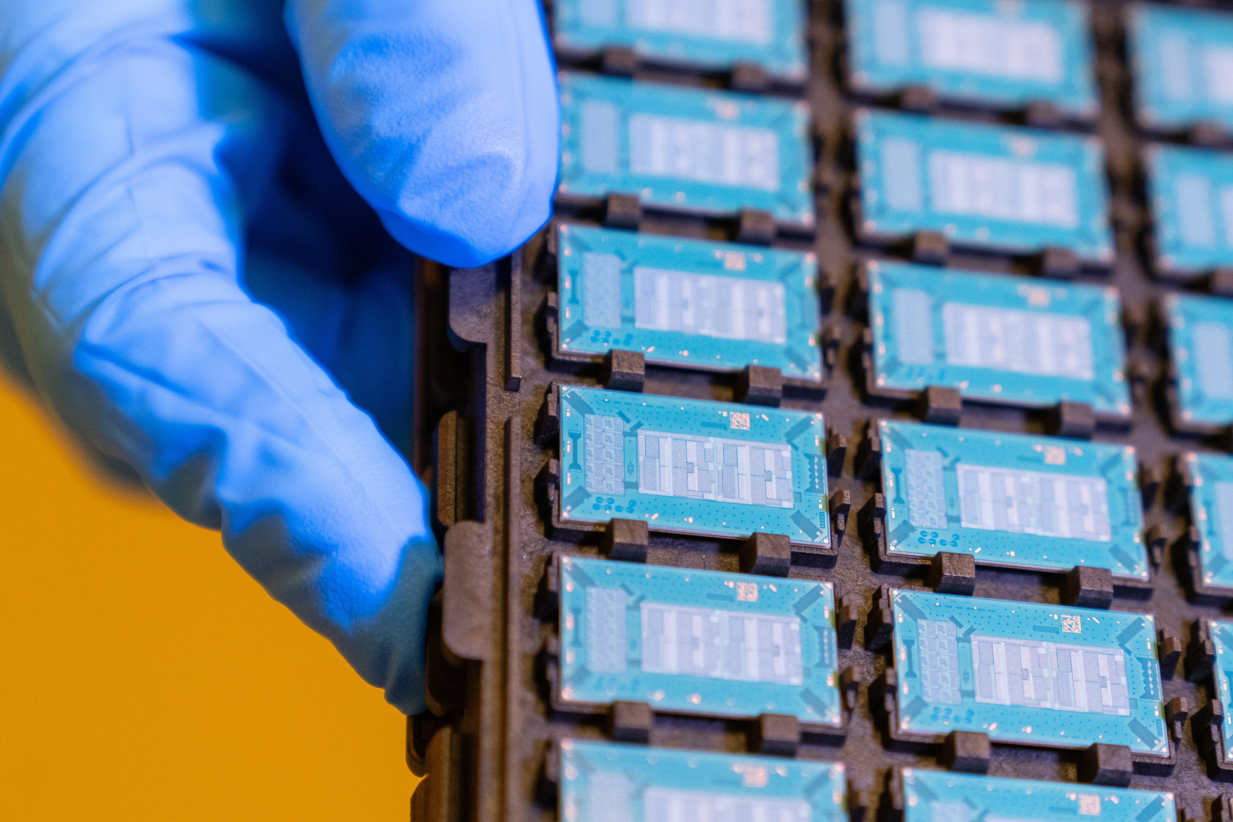
Assembled Check Chip Substrates
All of this, in flip, permits for not solely bigger chips, however for extra dies to be positioned on a same-sized chip. In accordance with Intel, glass packaging would permit them to position 50% extra dies on a chip – or reasonably, the die advanced space inside a chip may very well be 50% bigger – permitting for extra densely packed chips than what Intel can do right now.
Lastly, on {the electrical} facet of issues, glass core substrates, and extra particularly the TGVs, reportedly provide higher electrical efficiency as effectively. Owing to the low loss nature of the dielectric utilized in TGVs mixed with the a lot bigger variety of them, Intel says that cup core substrates will permit for cleaner sign routing and energy supply. Within the case of the previous, meaning having the ability to do 448G signaling via copper, reasonably than having to make use of optical interconnects. In the meantime, lower-loss energy supply would enhance general chip effectivity by that rather more, by lowering the quantity of vitality that’s misplaced as warmth earlier than it even reaches the processor dies.
Farther down the road nonetheless, glass core substrates must also make co-packaged optics simpler to perform for if you do need to use optical. A glass substrate would permit for optical interconnects to be built-in proper into the chip, reasonably than having to tack it on in different manners.
So if glass is so nice, what’s the catch? Whereas Intel is understandably extra excited to speak about what’s good about glass core substrates and what they’ve discovered works effectively so far, one inescapable factor will likely be price. Like all new know-how, glass core substrates will likely be costlier to provide and bundle with than tried and true (and low-cost) natural substrates. And whereas Intel isn’t speaking about yields this far out, will probably be arduous for glass to compete with natural, no less than at first.
Extra broadly talking, glass core substrates additionally signifies that Intel must bootstrap an entire ecosystem for the fabric. They aren’t vertically built-in with natural substrates right now, and so they received’t be vertically built-in with glass, both. To that finish, Intel is already working with companions right now to develop the required tooling and provide capability, to carry themselves to preliminary industrial manufacturing. However over the longer-term, Intel might want to work out the way to make outsourced testing and meeting attainable, particularly as Intel plans to supply glass core substrates to IFS prospects sooner or later.
Lastly, it bears noting that whereas glass core substrates permit for a tighter sign pitch than natural substrates, they don’t seem to be a substitute for EMIB, Foveros, or different extra superior packing methods primarily based round utilizing silicon mediums. A 75µm pitch for a TGV continues to be a far cry from the 45µm pitch of EMIB, by no means thoughts the <10µm pitch deliberate for Foveros Direct. So all of these packaging applied sciences will stay complementary add-ons to glass core substrates, at finest changing EMIB in fringe instances of merchandise that don’t want the complete density enhancements of EMIB.
Glass In Motion: Intel’s Totally Practical Check Chip
The ultimate a part of right now’s announcement from Intel relies across the manufacturing facet of issues. As famous earlier, Intel has been engaged on glass core substrates for over 10 years now, and extra not too long ago has been embarking on a three-and-a-half-year pathfinding mission to carry glass core substrates to the subsequent step. Backing these efforts, at this level the corporate has a completely built-in R&D line up and working in certainly one of their Chandler, Arizona fabs (the identical one which does EMIB). Altogether, Intel has spent over a billion {dollars} on glass core R&D so far.
The primary fruit of their R&D efforts, Intel has accomplished the meeting of a set of take a look at automobiles – multi-chip packages constructed over a glass substrate. The chips, which look much like Intel’s ultra-low energy cellular chips (Alder Lake-U 9W?), are reportedly totally practical, giving Intel some sensible outcomes to report on. Whereas we don’t have a ton of particulars on the chip, Intel has advised us that it makes use of 3 layers of RDL, and the TGVs have a pitch of 75µm.
Together with proving {the electrical} properties of glass, the small take a look at chip can also be meant to show a number of the bodily properties, as effectively. The glass core was made very thick – on the order of 1mm – as a way to show that TGVs would work with such a thick core. For the type of huge, high-end chips Intel is planning on utilizing glass core packing for, these chips would require a really thick core as a way to hit their measurement targets, so Intel wanted to show that TGVs would (nonetheless) work at such lengths.
Intel Glass Core Substrates: Coming Later This Decade
Wrapping issues up, right now’s announcement serves as a kick-off of kinds for Intel’s glass core substrate period. Following on their decade of R&D work and their pathfinding dash, Intel now believes they’re prepared to start planning for the transition to glass core substrates of their merchandise – albeit a transition that’s nonetheless a number of years out.
If Intel’s product improvement goes in response to plan, the corporate intends to start transport glass core merchandise later this decade. The primary merchandise to get the glass core substrate therapy can be their largest and most worthwhile merchandise, comparable to high-end HPC and AI chips. These are the merchandise most strained by way of natural substrates right now as a result of measurement limits these substrates impose, and people are the bounds intel believes would most profit from glass core packaging.
Longer-term, the plan is to waterfall down the know-how from HPC chips into smaller and smaller chips, till the know-how is accessible (and viable) for Intel’s rank and file client chips. The corporate could be very fast to notice that cup and natural substrates will co-exist for years to return – and, like previous transitions, there’ll probably nonetheless be chips utilizing natural substrates effectively after glass is launched – however the firm can also be optimistic that they’ll be capable to carry the prices of glass core substrates all the way down to parity with natural substrates, ultimately making it attainable to reap the advantages even in lower-priced processors.
And Intel received’t be holding the know-how to themselves, both. As a part of the corporate’s broader initiative to change into a world class contract foundry, Intel will likely be providing glass core substrates to IFS prospects in due time. Whereas it’s far too early to guess when that may be (even Intel merchandise could also be 6 years out), having the ability to provide glass packaging might give Intel an enormous leg up over its rivals, particularly for producing high-end, highly-profitable chips.
Above all else, it must be reiterated that there’s an excessive amount of work Intel nonetheless must do as a way to carry glass core substrates to the market. But when the corporate is profitable, then the swap to glass will usher within the type of main know-how transition that solely occurs each 15 to twenty years.