MIT researchers develop approach to develop nanoLEDs for XR use

July 11, 2023 – Researchers at Massachusetts Institute of Know-how (MIT) have developed a brand new approach for integrating halide perovskite nanocrystals into nanoscale gadgets. The approach permits for the exact development of nanoscale LEDs (nanoLEDs), which might have potential functions in augmented and digital actuality (AR/VR) shows.
Halide perovskites are a gaggle of supplies identified for his or her distinctive optoelectronic properties, making them ultimate for high-performance photo voltaic cells, lasers, and light-emitting diodes (LEDs).
Till now, integrating these supplies on the nanoscale has been difficult on account of their delicate nature and susceptibility to break throughout typical fabrication processes. To beat this hurdle, MIT researchers devised a way that permits for exact on-site development of particular person halide perovskite nanocrystals, with management over their location inside 50 nanometers (a sheet of paper is 100,000 nanometers thick).
In response to MIT, the progressive new technique allows not solely exact management over the nanocrystals’ placement but additionally permits for exact management over their measurement, which instantly impacts their traits and efficiency. By rising the fabric regionally with desired options, the necessity for typical lithographic patterning steps that might doubtlessly trigger injury is eradicated.
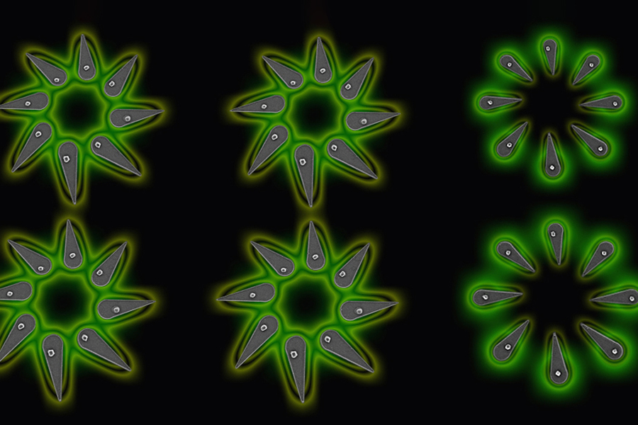
MIT famous that the approach is scalable, versatile, and suitable with typical fabrication steps, making it appropriate for integrating nanocrystals into practical nanoscale gadgets. Researchers efficiently utilized the strategy to manufacture arrays of nanoscale LEDs (nanoLEDs), which emit mild when electrically activated. These arrays have potential functions in optical communication and computing, lensless microscopes, quantum mild sources, and high-density, high-resolution shows for augmented and digital actuality.
The researchers’ method concerned making a nanoscale template with small wells that include the chemical course of by means of which crystals develop. By modifying the template’s floor and the within of the wells, researchers have been in a position to management a property referred to as “wettability,” guaranteeing that the answer containing the perovskite materials stays confined inside the wells.
The form of those wells performs a essential function in figuring out the nanocrystal positioning. By altering the nicely’s form, researchers have been in a position to engineer nanoscale forces that allow preferential placement of the crystals at desired places. Moreover, they found that they might exactly management the scale of the crystals by adjusting the scale of the wells.
“As our work reveals, it’s essential to develop new engineering frameworks for integration of nanomaterials into practical nanodevices. By shifting previous the normal boundaries of nanofabrication, supplies engineering, and machine design, these strategies can permit us to control matter on the excessive nanoscale dimensions, serving to us notice unconventional machine platforms vital to addressing rising technological wants,” mentioned Farnaz Niroui, the EE Landsman Profession Improvement Assistant Professor of Electrical Engineering and Laptop Science (EECS), a member of the Analysis Laboratory of Electronics (RLE), and senior creator of a brand new paper that describes the work.
The analysis findings have been revealed in Nature Communications, with the interdisciplinary effort involving researchers from electrical engineering, laptop science, and chemical engineering. The work was supported, partly, by the Nationwide Science Basis and the MIT Middle for Quantum Engineering.
MIT said that the analysis staff plans to discover additional functions for these tiny mild sources and take a look at the boundaries of miniaturization with the intention to successfully incorporate them into quantum methods. Past nanoscale mild sources, the method additionally opens up different alternatives for creating halide perovskite-based on-chip nanodevices, in keeping with MIT.
For the complete publish on the analysis announcement, click on here.
Picture credit score: MIT
Sam Sprigg
Sam is the Founder and Managing Editor of Auganix. With a background in analysis and report writing, he has been overlaying XR business information for the previous 5 years.