TSMC Opens Superior Backend Packaging Fab for AI and HPC Merchandise
TSMC on Friday formally opened its Superior Backend Fab 6 facility, which it is going to be utilizing to broaden the corporate’s capability for constructing high-end, multi-chiplet merchandise. The ability is alleged to be the primary all-in-one automated fab providing 3DFabric integration of front-end to back-end course of and testing providers.
TSMC’s Superior Backend Fab 6 can course of about a million 300-mm wafers per 12 months in addition to greater than 10 million hours of testing per 12 months. The manufacturing facility occupies 14.3 hectares in Zhunan Science Park and has a cleanroom that’s bigger than the mixed cleanroom areas of all different TSMC superior backend fabs, making it TSMC’s largest superior packaging facility so far, in accordance with the corporate.
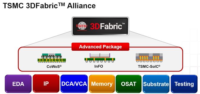
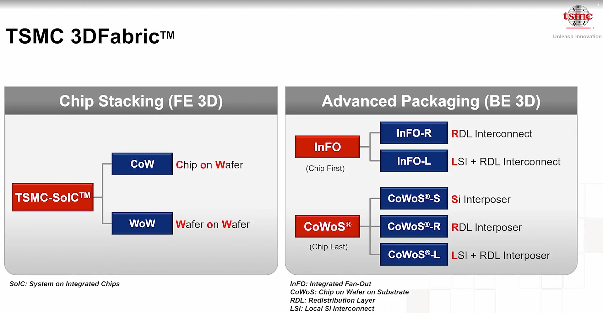
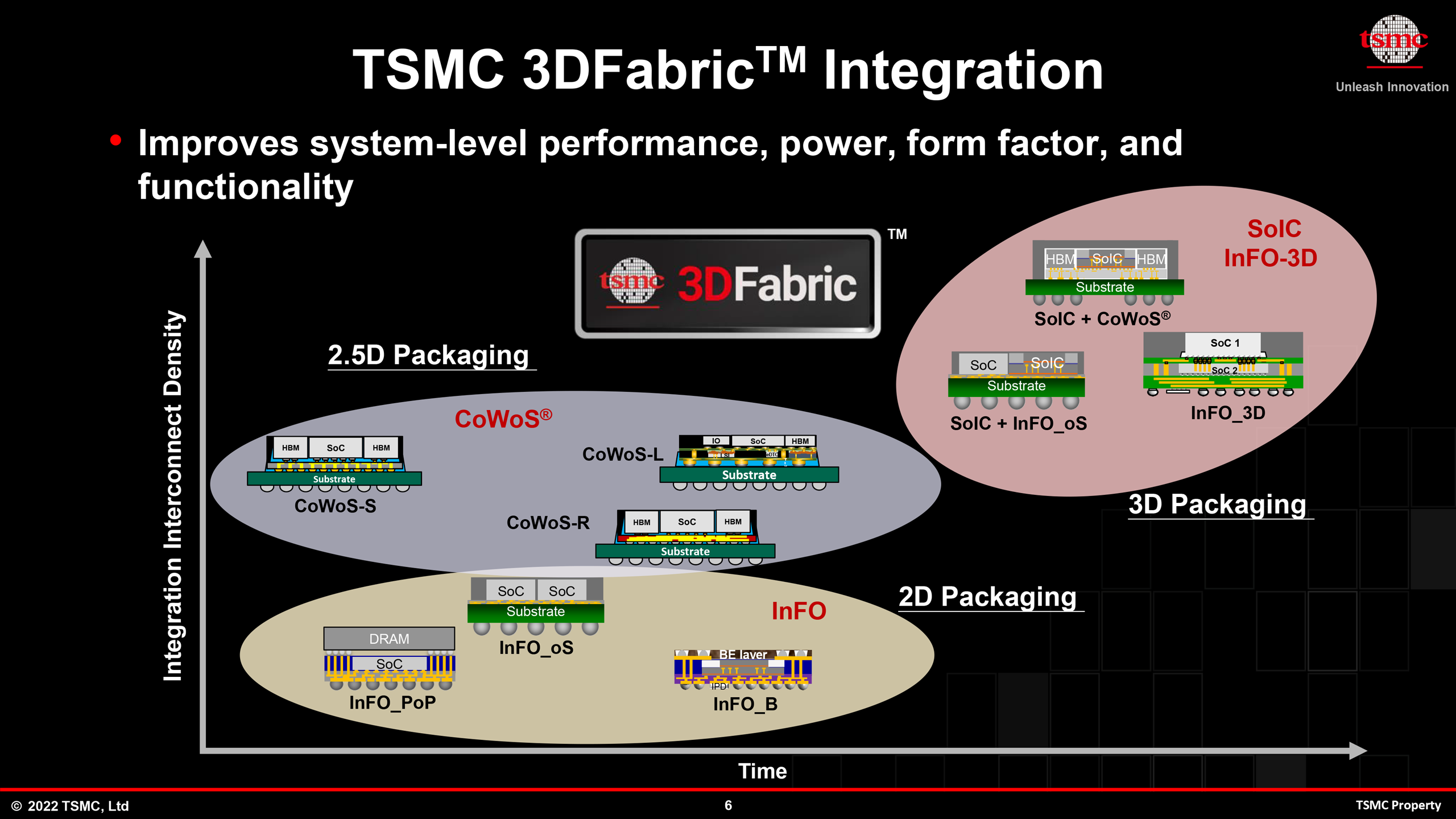
TSMC mentioned that its Superior Backend Fab 6 is prepared for mass manufacturing of TSMC-SoIC (System on Built-in Chips) course of expertise, which incorporates such frontend 3D stacking strategies as chip-on-wafer (CoW) and wafer-on-wafer (WoW). The fab can also be designed to deal with superior backend packaging applied sciences, equivalent to built-in fan-out (InFO) and chip-on-wafer-on-substrate (CoWoS) which are used for chips like Apple’s M2 Extremely, AMD’s Intuition MI300, and NVIDIA’s A100 and H100.
“Chiplet stacking is a key expertise for enhancing chip efficiency and cost-effectiveness. In response to the robust market demand for 3D IC, TSMC has accomplished early deployment of superior packaging and silicon stacking expertise manufacturing capability, and presents expertise management via the 3DFabric platform,” mentioned Dr. Jun He Vice President, Operations / Superior Packaging Know-how & Service, and High quality & Reliability.
Maybe probably the most notable characteristic of TSMC’s Superior Backend Fab 6 is complete five-in-one clever automated materials dealing with system that spans over 32 kilometers. The manufacturing info, ranging from the wafer stage to the die, is built-in with dispatching techniques to hurry up the manufacturing cycle. This course of is augmented with AI to hold out exact course of management and real-time defect detection to maximise yields. That is notably necessary as whenever you bundle a multi-chiplet answer like AMD’s MI300 any abnormality on the bundle stage instantly invalidates all of the chiplets which are on it inflicting a loss that prices at the very least hundreds of {dollars}. The fab’s information processing functionality per second is 500 instances that of a typical front-end fab, which permits a radical manufacturing historical past for every die and permits the foundry to hint every die it processes on the fab.
“With the manufacturing capability that meets our prospects’ wants, we’ll unleash innovation collectively and grow to be an necessary associate that prospects belief in the long run,” added Jun He.