TSMC Preps 6x Reticle Dimension Tremendous Provider Interposer for Excessive SiP Processors
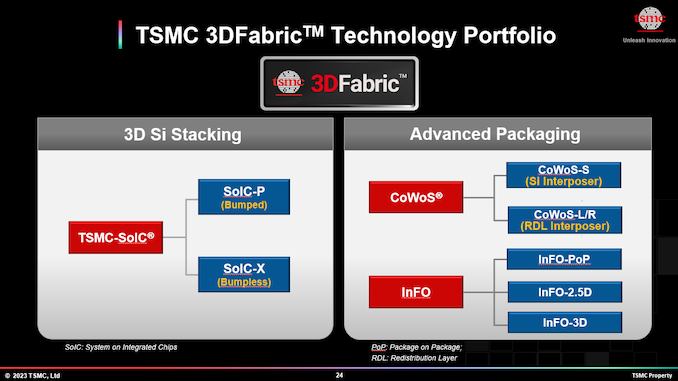
As a part of their efforts to push the boundaries on the biggest manufacturable chip sizes, Taiwan Semiconductor Manufacturing Co. is engaged on its new Chip-On-Wafer-On-Substrate-L (CoWoS-L) packaging technology that can enable it to construct bigger Tremendous Provider interposers. Aimed on the 2025 time span, the following technology of TSMC’s CoWoS know-how will enable for interposers reaching as much as six occasions TSMC’s most reticle measurement, up from 3.3x for his or her present interposers. Such formidable system-in-packages (SiP) are meant to be used by performance-hungry information heart and HPC chips, a distinct segment market that has confirmed keen to pay important premiums to have the ability to place a number of excessive efficiency chiplets on a single package deal.
“We’re at present growing a 6x reticle measurement CoWoS-L know-how with Tremendous Provider interposer know-how,” mentioned mentioned Yujun Li, TSMC’s director of enterprise improvement who’s in control of the foundry’s Excessive Efficiency Computing Enterprise Division, on the firm’s European Know-how Symposium 2023.
World megatrends like synthetic intelligence (AI) and high-performance computing (HPC) have created demand for seemingly infinite quantities of compute horsepower, which is why firms like AMD, Intel, and NVIDIA are constructing extraordinarily advanced processors to handle these AI and HPC functions. One of many methods to extend compute capabilities of processors is to extend their transistor rely; and to take action effectively nowadays, firms use multi-tile chiplet designs. Intel’s spectacular, 47 tile Ponte Vecchio GPU is an efficient instance of such designs; however TSMC’s CoWoS-L packaging know-how will allow the foundry to construct Tremendous Provider interposers for much more gargantuan processors.
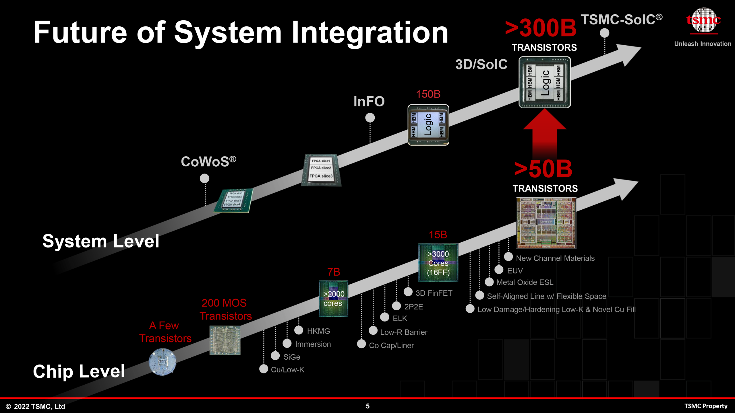
The theoretical EUV reticle restrict is 858mm2 (26 mm by 33 mm), so six of those masks would allow SiPs of 5148 mm2. Such a big interposer wouldn’t solely afford room for a number of giant compute chiplets, nevertheless it additionally leaves loads of room for issues like 12 stacks of HBM3 (or HBM4) reminiscence, which implies a 12288-bit reminiscence interface with bandwidth reaching as excessive as 9.8 TB/s.
“The Tremendous Provider interposer options a number of RDL layers on the entrance in addition to on the bottom of the interposer for yield and manufacturability,” defined Li. “We will additionally combine numerous passive elements within the interpreter for efficiency. This six reticle-size CoWoS-L might be certified in 2025”
Constructing 5148 mm2 SiPs is a particularly robust duties and we are able to solely surprise how a lot they may price and the way a lot their builders will cost for them. At current NVIDIA’s H100 accelerator, whose packaging spans an interposer a number of reticles in measurement, prices round $30,000. So a substantial bigger and extra highly effective chip would possible push costs larger nonetheless.
However paying for the price of giant processors is not going to be the one big investments that information heart operators might want to make. The quantity of energetic silicon that 5148 mm2 SiPs can home will virtually actually lead to a few of the most power-hungry HPC chips produced but – chips that will even want equally highly effective liquid cooling to match. To that finish, TSMC has disclosed that it has been testing on-chip liquid cooling know-how, stating that it has managed to chill down silicon packages with energy ranges as excessive as 2.6 kW. So TSMC does have some concepts in thoughts to deal with the cooling want of those excessive chips, if solely on the worth of integrating much more cutting-edge know-how.