Samsung Kicks Off DDR5 DRAM Manufacturing on 12nm Course of Tech, DDR5-7200 within the Works
Samsung on Thursday stated it had began excessive quantity manufacturing DRAM chips on its newest 12nm fabrication course of. The brand new manufacturing node has allowed Samsung to scale back the facility consumption of its DRAM units, in addition to lower their prices considerably in comparison with its previous-generation node.
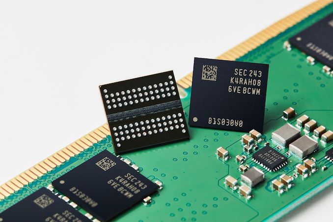
In response to Samsung’s announcement, the corporate’s 12nm fabrication course of is getting used to supply 16Gbit DDR5 reminiscence chips. And whereas the corporate is already producing DDR5 chips with that capability (e.g. K4RAH086VB-BCQK), the change to the newer and smaller 12nm course of has paid off each by way of energy consumption and die measurement. As in comparison with DDR5 dies made on the corporate’s previous-generation node (14nm), the brand new 12nm dies supply as much as 23% decrease energy consumption, and Samsung is ready to produce 20% extra dies per wafer (i.e., the DDR5 dies are tangibly smaller).
Samsung says that the important thing innovation of its 12nm DRAM fabrication course of is utilization of latest high-k materials for DRAM cell capacitors that enabled it to extend cell’s capacitance to spice up efficiency, however with out growing their dimensions and die sizes. Greater DRAM cell capacitance means a DRAM cell can retailer extra information and cut back power-draining refresh cycles, therefore growing efficiency. Nevertheless, bigger capacitors usually end in elevated cell and die measurement, which makes the ensuing dies dearer.
DRAM makers have been addressing this through the use of high-k supplies for years, however discovering these supplies is getting trickier with every new node as reminiscence makers additionally must take into consideration yields and manufacturing infrastructure they’ve. Apparently, Samsung has succeeded in doing so with its 12nm node, although it doesn’t make any disclosures on the matter. That Samsung has succeeded in decreasing their die measurement by a significant quantity in any respect is sort of outstanding, as analog elements like capacitors have been a number of the first components of chips to cease cutting down additional with finer course of nodes.
Along with introducing a brand new high-k materials, Samsung additionally lowered working voltage and noise for its 12nm DDR5 ICs to supply a greater stability of efficiency and energy consumption in comparison with predecessors.
One of many facets about Samsung’s 12nm DRAM expertise is that it appears to be like to be the corporate’s 3rd Era manufacturing node for reminiscence that makes use of excessive ultraviolet lithography. The primary D1x node was purely designed as a proof of idea and its successor D1a, which has been in use since 2021, used EUV for 5 layers. In the meantime, it’s unclear to what diploma Samsung’s 12nm node is utilizing EUV instruments.
“Utilizing differentiated course of expertise, Samsung’s industry-leading 12nm-class DDR5 DRAM delivers excellent efficiency and energy effectivity,” stated Jooyoung Lee, Government Vice President of DRAM Product & Know-how at Samsung Electronics.
In the meantime, Samsung can also be eyeing sooner reminiscence speeds with their new 12nm DDR5 dies. In response to the corporate, these dies can run as quick as DDR5-7200 (i.e. 7.2Gbps/pin), which is effectively forward of what the official JEDEC specification presently permits for. The voltage required is not being acknowledged, but when nothing else, it gives some promise for future XMP/EXPO reminiscence kits.