1Tb TLC with 3.2 GT/s IO Velocity
Kioxia and Western Digital formally launched their 8th Technology BiCS 3D NAND reminiscence with 218 lively layers. The brand new storage machine presents a 1Tb capability in 3D TLC mode and options 3200 MT/s knowledge switch velocity, a mixture that may allow SSD makers to construct high-performance, high-capacity drives. To allow such an excessive interface velocity, the businesses adopted an structure akin to YMTC’s Xtacking.
The 218-layer BiCS 3D NAND machine collectively developed by Kioxia and Western Digital helps triple-level cell (TLC) and quad-level cell (QLC) configurations to maximise storage density and develop addressable purposes. The businesses mentioned that the brand new machine embraces their new ‘lateral shrink know-how to extend bit density by over 50’ with out elaborating. Contemplating that the flash reminiscence IC elevated the variety of lively layers by 34%, the declare a few 50% bit density improve signifies that builders additionally shrank lateral sizes of NAND cells to slot in extra of them per layer.
In the meantime, the 218-layer 3D NAND machine contains a quad-plane structure permitting for the next degree of parallelism for programming and skim instances and elevated efficiency. As well as, the 218-layer 3D TLC machine additionally has a 3200 MT/s (which may present a 400 MB/s peak learn/write velocity) enter/output interface, which is the very best I/O velocity introduced to date. Excessive knowledge switch charges can be helpful for high-end consumer and enterprise SSDs that includes a PCIe 5.0 interface.
The important thing innovation of the 8th Technology BiCS 3D NAND reminiscence is the all-new CBA (CMOS immediately Bonded to Array) structure that implicates separate manufacturing of 3D NAND cell array wafers and I/O CMOS wafers utilizing essentially the most optimum course of applied sciences after which bonding them collectively to create a ultimate product that provides elevated bit density and quick NAND I/O velocity. In the meantime, Kioxia and Western Digital should disclose particulars about their CBA structure and whether or not the I/O CMOS wafers carry different NAND peripheral circuitry, like web page buffers, sense amplifiers, and cost pumps.
Producing reminiscence cells and peripheral circuits individually solves a number of issues because it permits producers to make them utilizing essentially the most environment friendly course of applied sciences of their sections of cleanrooms. This brings additional advantages because the business adopts strategies like string stacking.

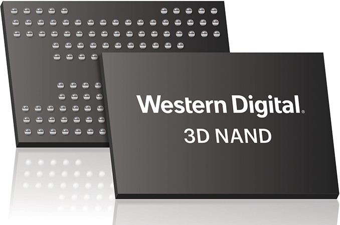
Kioxia and Western Digital Fab 7, Yokkaichi Plant, Japan
Kioxia mentioned it had began pattern shipments of 8th Technology BiCS 3D NAND reminiscence gadgets to pick prospects. Nonetheless, there isn’t a phrase when the corporate expects to provoke quantity manufacturing of its next-generation flash reminiscence. It’s not uncommon for firms to announce new sorts of 3D NAND quarters earlier than they enter mass manufacturing, so it’s cheap to count on 8th Gen BICS available on the market in 2024.
“By our distinctive engineering partnership, we’ve efficiently launched the eighth-generation BiCS Flash with the business’s highest bit density,” mentioned Masaki Momodomi, Chief Know-how Officer at Kioxia Company. “I’m happy that Kioxia’s pattern shipments for restricted prospects have began. By making use of CBA know-how and scaling improvements, we have superior our portfolio of 3D flash reminiscence applied sciences to be used in numerous data-centric purposes, together with smartphones, IoT gadgets, and knowledge facilities.“