Synopsys Intros AI-Powered EDA Suite to Speed up Chip Design and Lower Prices

Synopsys has launched the business’s first full-stack AI-powered suite of digital design automation instruments that covers all levels of chip design, from structure to design and implementation to manufacturing. The Synopsys.ai suite guarantees to radically scale back improvement time, decrease prices, enhance yields, and improve efficiency. The set of instruments is ready to be extraordinarily helpful for chips set to be made on modern nodes, corresponding to 5nm, 3nm, 2nm-class, and past.
Chip Design Challenges
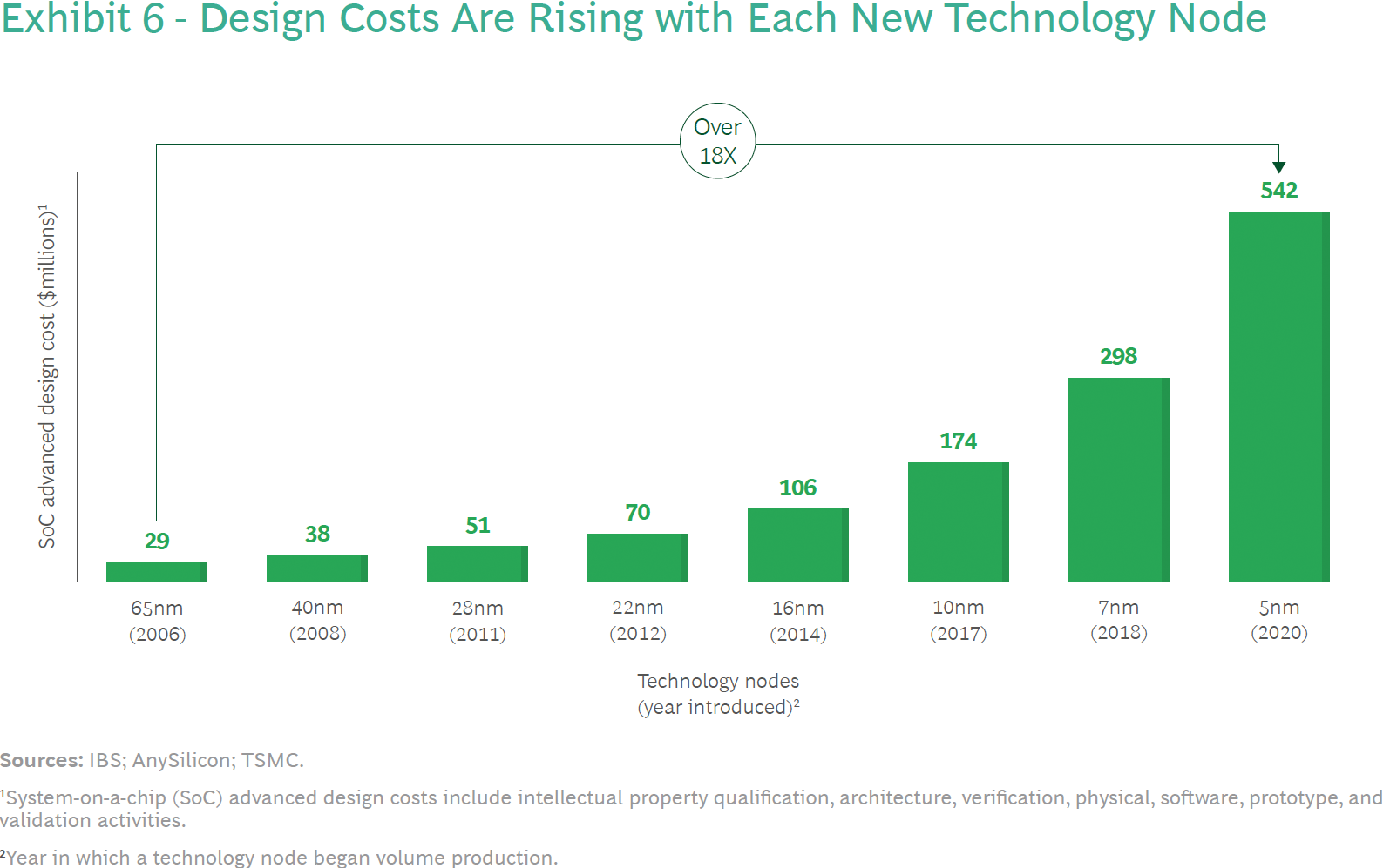
As chips acquire complexity and undertake newer course of applied sciences, their design and manufacturing prices escalate to unprecedented ranges. Designing a fairly advanced 7 nm chip prices about $300 million (together with ~ 40% for software program). In distinction, the design price of a sophisticated 5 nm processor exceeds $540 million (together with software program), in line with International Business Strategies (IBS) estimates. At 3 nm, a fancy GPU will price about $1.5 billion to develop, together with circa 40% for software program.
The normal ‘waterfall’ semiconductor design method is maybe one of many the reason why chip improvement prices skyrocket so quickly. It takes tons of (if not hundreds) of engineers and hundreds of servers over a number of years to develop and simulate architectural, structural, logic, and structure designs. In the meantime, each design stage entails duties which are important for the standard of the chip, however they’re iterative and time-consuming in nature. For apparent causes, as chips get extra advanced, every design change will get longer as firms can not throw in as many engineers as they need to a given process as a result of the variety of individuals they’ve is restricted.
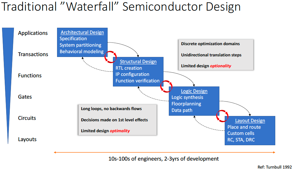
Issues get more difficult because the waterfall method virtually excludes backward flows, so individuals implementing one of many hundreds of attainable place and route designs have little to zero affect on the architectural or structural design. Consequently, the one approach to keep away from inefficiencies leading to higher-than-expected prices, lower-than-expected efficiency, and/or higher-than-expected energy consumption is to make totally different design groups work nearer collectively in any respect levels. But, this will get tougher as design cycles get longer.
Manufacturing prices at 5 nm and three nm manufacturing nodes are additionally noticeably increased than these on previous-generation fabrication applied sciences. The most recent modern manufacturing processes extensively use excessive ultraviolet lithography and costlier uncooked supplies (e.g., pellicles for photomasks, resists, and so on.). Subsequently, it will get much more essential for chip builders to construct close-to-perfect designs which are cheaper to make.
Generally, the semiconductor business faces a number of challenges as of late because it wants to chop down improvement time, preserve (and even scale back) chip improvement prices, and guarantee predictable manufacturing prices. All the pieces needs to be performed when the business faces a deficit of extremely expert engineers.
That is the place the Synopsys.ai EDA suite comes into play.
From Scratch to Excessive-Quantity Manufacturing
The Synopsys.ai full-stack EDA suite consists of three key purposes the DSO.ai AI for chip design: the Synopsys VSO.ai for purposeful verification, and the TSO.ai for silicon check. The suite is designed to hurry up iterative and time-consuming chip design levels utilizing machine studying and reinforcement studying accelerated by trendy CPUs and GPUs.
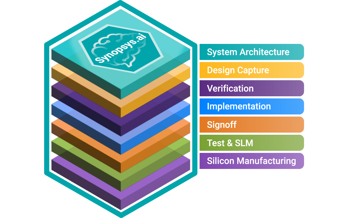
Synopsys has been providing its DSO.ai place and route AI-driven solution for about two years now, and over 100 designs have been taped out utilizing the EDA instrument up to now. However this time round, the corporate is taking a look at fast-tracking all design levels with AI. The software program suite can be utilized in any respect levels, together with simulations, design seize, IP verification, bodily implementation, signoff, check, and manufacturing.
Higher Architectures Delivered Quicker
Small teams of very proficient engineers sometimes develop microarchitectures, and this stage is taken into account by many as an intersection of know-how and artwork. In reality, microarchitectures are developed pretty shortly too. Synopsys says that even this stage will be accelerated and improved with AI as synthetic as, in contrast to individuals, machines can shortly estimate essentially the most environment friendly structure parameters and knowledge paths.
The Common Supervisor of Synopsys’s Digital Design Automation Group (EDA), Shankar Krishnamoorthy, states, “The entire strategy of creating a chip begins with the structure of the chip and there are loads of choices to be made there,” He additionally went on to say “How massive does your cache should be? What sort of interfaces run between your laptop and reminiscence? What configurations of reminiscence do you have to take into account, so there are lots of, many decisions there, which an structure skilled would discover quickly, after which converge on what are the precise parameters to implement the chip with. In order that course of itself is one thing the place AI can be utilized to quickly discover that answer area […] and produce a good higher end result that they might not have gotten to, simply due to the compute energy that AI can work with.“
One other facet of utilizing AI for microarchitectural explorations is boosting the microarchitecture improvement capabilities of a given firm amid shortages of skilled architects.
Shankar Krishnamoorthy additionally stated, “In instances when you’ve got an skilled architect already there, AI is basically an assistant. The trendy AI strategies are actually good at zooming in on the areas of curiosity in a really massive parameter area through the use of rewards and penalties. Then you definately [end up with] a set of menu of decisions (corresponding to tradeoffs between energy and efficiency) from which the architect type of picks the very best one for the workload of curiosity.“
Dashing Up IP Verification
Useful and IP verification is a chip design step that takes up loads of time. It’s crucial to check every IP individually and be certain that it capabilities appropriately earlier than integrating them, because the complexity of verification will increase exponentially when a number of IPs are mixed. In the meantime, it’s essential to reaching a excessive stage of check protection for every particular person IP.

These days, the widespread method for verifying IP entails the designer making a check benchmark that displays their verification technique. This check benchmark is then simulated utilizing typical simulation strategies, corresponding to constrained random simulation, with the assistance of a conventional simulator. Attaining excessive goal protection for a given IP sooner is a problem that may be addressed by the Synopsys VSO.ai, which is a part of Synapsys.ai.
“By embedding strategies like reinforcement studying deep into the simulation engine, you possibly can obtain that focus on protection” stated the pinnacle of Synopsys’s EDA group. “You say, I want 99% protection of this IP, you possibly can obtain that focus on protection in a a lot shorter time frame, and utilizing a lot fewer simulations, as a result of basically, that reinforcement studying engine that’s embedded into the simulation engine is consistently [communication] with the engine that’s producing the stimulus.”
Renesas confirmed that the Synapsys VSO.ai software program may each develop goal protection and pace up the IP verification course of.
Takahiro Ikenobe, who’s the IP Improvement Director of the Shared R&D Core IP Division at Renesas, stated, “Assembly high quality and time-to-market constraints is quick changing into troublesome utilizing conventional human-in-the-loop strategies because of the ramp in design complexity. Utilizing AI-driven verification with Synopsys VSO.ai, a part of Synopsys.ai, we’ve achieved as much as 10x enchancment in decreasing purposeful protection holes and as much as 30% improve in IP verification productiveness demonstrating the flexibility of AI to assist us deal with the challenges of our more and more advanced designs.“
Place and Route Accomplished Quick
Talking of more and more advanced designs, we should keep in mind how exhausting it’s to appreciate the trendy processor’s design bodily. Whereas trendy EDA instruments streamline chip improvement, expert human engineers are nonetheless required to effectively implement chip floorplan, structure, placement, and routing, using their expertise to create environment friendly designs. Though skilled engineers sometimes work quick, they’re restricted of their skill to judge tons of of design choices, discover all potential mixtures, and simulate tens and even tons of of various layouts to determine the optimum design inside an inexpensive timeframe. Consequently, in lots of instances, they implement their best-known methodologies, which might not be essentially the most environment friendly ones for a specific chip made on a specific manufacturing node.

That is after they can use the Synopsys DSO.ai platform that doesn’t must simulate all of the attainable methods to put and route a chip however leverages synthetic intelligence to judge all mixtures of architectural decisions, energy and efficiency targets, geometries after which simulate a number of totally different layouts to seek out the one which complies with desired efficiency, energy, space, and price (PPA) mixture in a fraction of the time.
Talking of simulation, it is very important observe that simulating a bodily massive chip (whether or not a CPU, GPU or a reminiscence IC) is relatively exhausting to perform. Historically chip designers used massive machines based mostly on CPUs or FPGAs to simulate future chips. Nonetheless, just lately Synopsys utilized GPU acceleration for these workloads and acquired a several-fold efficiency uplift.
“If we have a look at the design of discrete reminiscence, like DRAM or NAND flash, these are very massive circuits that should be simulated for electrical correctness, bodily correctness, you already know, stress, IR drop all the opposite varieties of results,” Krishnamoorthy informed us. “Simulation of those very massive discrete reminiscence constructions could be very time-consuming. That is an space the place we’ve efficiently utilized GPU acceleration with a view to obtain several-fold acceleration of the time it takes to simulate these massive circuits.”
One of many fascinating issues that Synopsys talked about throughout our dialog is that the DSO.ai instrument can be utilized to implement analog circuits — which barely (if in any respect) scale with every new node — in accordance with new design guidelines.
“Basically, in the event you take a PLL, otherwise you take some other kind of analog circuit, and you might be actually not altering the circuit itself, you might be migrating it from, for instance, 7 nm to five nm or 5 nm to three nm,” defined the Synopsys government. “That strategy of migrating a circuit from one node to a different is one thing that’s ripe for automation and ripe for the applying of AI. So that’s one other space the place we’ve utilized AI to speed up that course of and minimize down the time and effort wanted emigrate analog circuits by a big quantity.“
In line with Synopsys, comparable AI capabilities can simplify the duty of transferring chip designs between various foundries or course of nodes. Nonetheless, it’s price contemplating that intricate designs’ energy, efficiency, and space traits (PPAc) are custom-made for particular nodes. It stays unsure whether or not AI can successfully migrate such a design from one foundry to a different whereas preserving all the important thing traits and whether or not potential trade-offs of such a migration might be vital.
Synopsys has been providing its DSO.ai platform for about a few years, and by now, about 170 chip designs applied utilizing this EDA instrument have been taped out.
“We talked about crossing the 100 tape out milestone in January,” stated Krishnamoorthy. “We’re near 170 now, so the tempo of adoption of that AI-based bodily design is basically quick among the many buyer base.“
Take a look at and Silicon Lifecycle Administration
After a chip was applied and produced, chip designers must confirm that every thing works high-quality in a course of that’s considerably just like IP verification. This time round, no simulations are concerned. As an alternative, a chip is inserted right into a tester machine, and particular check patterns are run to verify that the chip is working appropriately. Subsequently, the variety of patterns required to check an SoC or an precise system is a serious concern for product engineering departments.
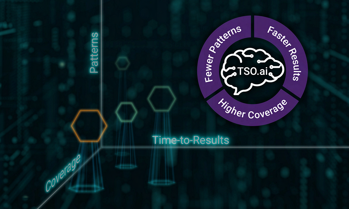
The Synopsys TSO.ai instrument is designed to assist semiconductor firms generate the precise check patterns, minimize the variety of patterns they should run by 20% to 30% and pace up the silicon check/verification section. The identical check sequences are then used to check all mass-produced chips to make sure they perform appropriately. The length of the testing section instantly impacts prices, so it’s notably essential, particularly for high-volume components.
“Now we have proven how AI can minimize down the overall variety of patterns wanted with a view to check circuits by a big quantity,” stated the Synopsys government. “We’re speaking about 20% to 30% kind of reductions in check patterns. In order that instantly interprets to price of check and time on the tester, which is a giant deal for firms.“
Make Chip Designs Cheaper
Utilizing AI-enabled instruments in chip improvement can pace up their time to market and scale back their improvement and manufacturing prices considerably. Relying on the precise design, Synopsys says we’re taking a look at, at the least a 30% – 40% vary, and now that {hardware} improvement prices of advanced chips attain $325 million (at 5 nm) – $900 million (at 3 nm), we’re speaking about some huge cash.
“Chip prices are clearly exhausting to estimate,” stated Shankar Krishnamoorthy. “If I needed to guess, I might say, [cost reduction from AI tools usage is] undoubtedly within the 30% to 40% vary.“
Usually, engineering prices account for round 60% of a chip design price, whereas compute prices account for about 40%. AI can be utilized to cut back each sorts of prices, in line with Synopsys.
When a longtime firm designs a brand new chip, it contains 30% to 40% of recent IP and 60% to 70% of seasoned IP, stated Krishnamoorthy. Historically, many engineers migrate IPs from the earlier node to the following node, typically porting over 60% to 70% of the IPs with minor modifications. Nonetheless, that is an inefficient use of assets. As an alternative, by leveraging AI to use earlier learnings to the following era, the time and assets required to finish these incremental blocks will be dramatically decreased, permitting human engineers to expedite the method.
Relating to new IP blocks, figuring out one of the best ways to architect and implement them will be difficult and unsure, typically requiring at the least one engineer per block. This method can affect the variety of individuals wanted for the challenge to converge. Nonetheless, leveraging AI as an assistant can quickly discover and study new designs and architectures to find out the optimum technique for implementation, verification, and testing. This will considerably scale back the funding wanted for brand spanking new blocks.
Lastly, deploying DSO.ai, VSO.ai, and TSO.ai extra broadly can scale back the compute price by enabling extra clever runs of EDA instruments. Moderately than counting on a trial-and-error method and indiscriminately simulating all types of circuits, focused AI-enabled runs can be utilized to attain comparable outcomes. In the long run, compute prices will lower.
Abstract
Synopsys.ai is the business’s first suite of EDA instruments that may deal with all phases of chip design, together with IP verification, RTL synthesis, flooring planning, place and route, and ultimate purposeful verification.

The utilization of machine studying and reinforcement studying enabled for time-consuming and iterative designed levels corresponding to design area exploration, verification protection, regression analytics, and check program era, guarantees to cut back design prices, decrease manufacturing prices, improve yields, enhance efficiency, and scale back time-to-market. The set of instruments will be notably helpful for chips set to be made on modern nodes, corresponding to 5nm, 3nm, 2nm-class, and past.
Moreover, offloading among the duties to AI-enabled EDA instruments can considerably lower the load on engineering groups, releasing up their time and minds to develop new options, improve product differentiation, or design extra chips, in line with Synopsys.
The corporate says that prime chip designers already use its Synopsys.ai, although not all chips are designed with AI help for now.
One of many fascinating issues that Synopsys identified is that its Synapsys.ai software program suite largely depends on CPU acceleration for AI. Whereas choose issues like massive circuit simulations will be accelerated utilizing GPUs, many of the workloads run on Intel CPUs.