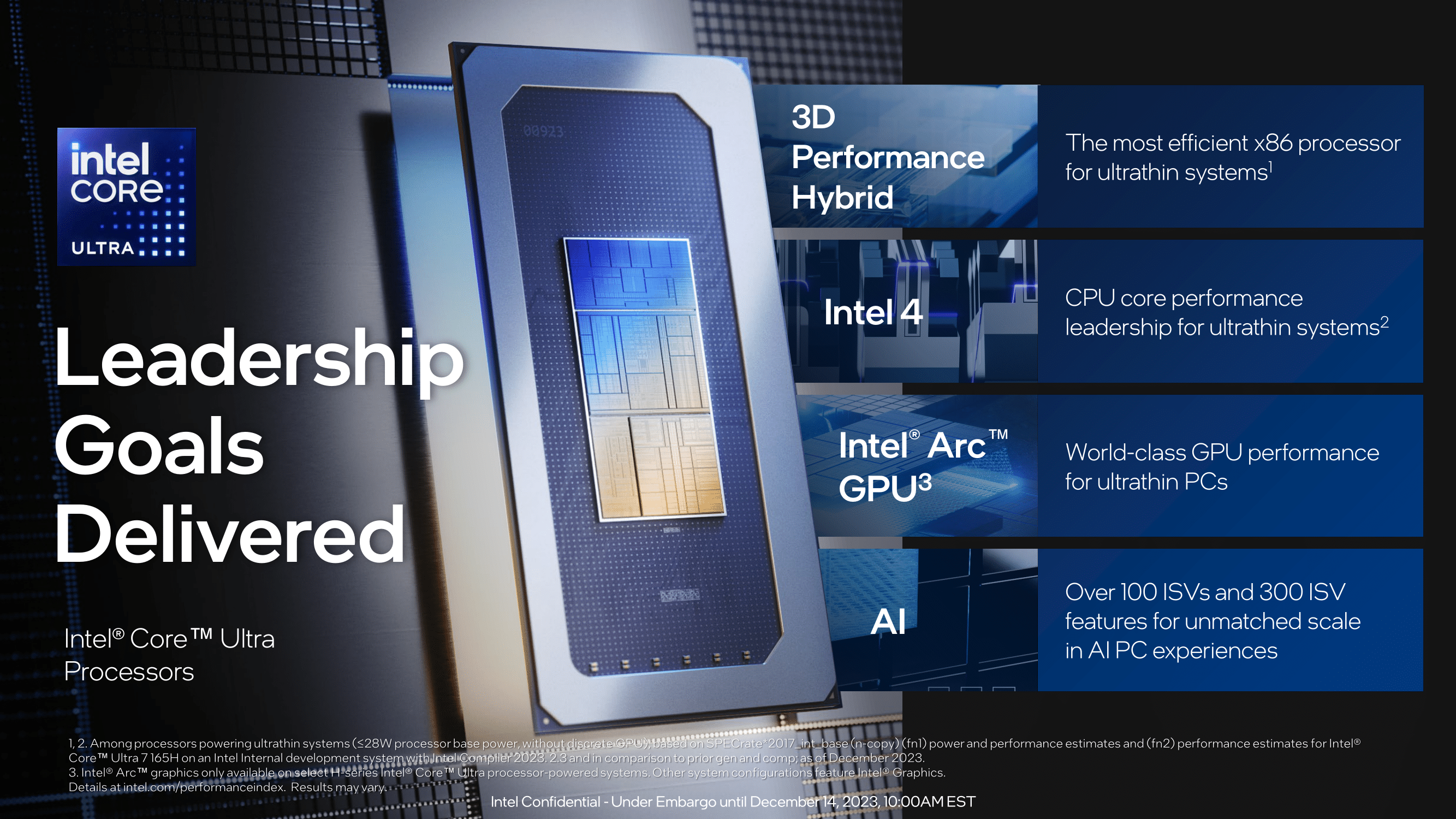
Meteor Lake Brings AI and Arc to Extremely Skinny Notebooks
Intel has launched their first cellular processors based mostly on their extremely anticipated Meteor Lake platform, the Core Extremely H and the Core Extremely U sequence. Accessible in the present day, the Extremely Core H sequence has 4 SKUs, together with two Extremely 7 16 core (6P+8E+2LP) chips and two 14 core (4P+8E+2LP) Extremely 5 chips. All run at a base TDP of 28 W, with a most turbo TDP of as much as 115 W. The Core Extremely-H sequence is designed for ultra-portable notebooks however presents extra efficiency in each computing and graphics inside a slimline package deal.
Additionally introduced is the Intel Core Extremely U-series, which incorporates 4 15/57 W (base/turbo) SKUs, with two Core Extremely 7 and two Core Extremely 5 SKUs, and all coming with a variance in P, E-core and Intel’s newest built-in Arc Xe graphics frequencies. All of Intel’s introduced Core Extremely U-series processors for cellular function 10 CPU cores, with two Efficiency cores and eight Effectivity cores, making them perfect for lower-powered and ultra-thin notebooks.
The launch of Intel’s tile-based Meteor Lake SoC marks step one in a sequence of power-efficient and AI-focused chips on Intel 4 for the cellular market, which is in the end designed to cater to the rising must make the most of AI inferencing on-chip. Each the Intel Core Extremely H and U households of chips embody two new Low Energy Island (LP-E) cores for low insensitive workloads, with two Neural Compute Engines inside the Intel AI NPU designed to sort out generative AI inferencing.
Intel Core Extremely Processors: Rapidly Recapping Meteor Lake
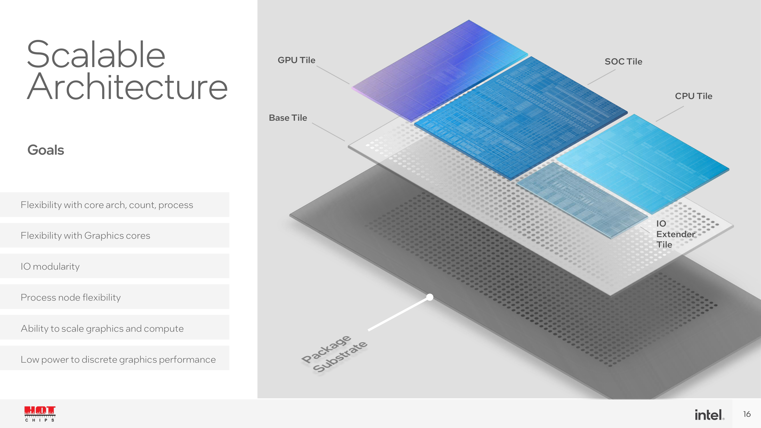
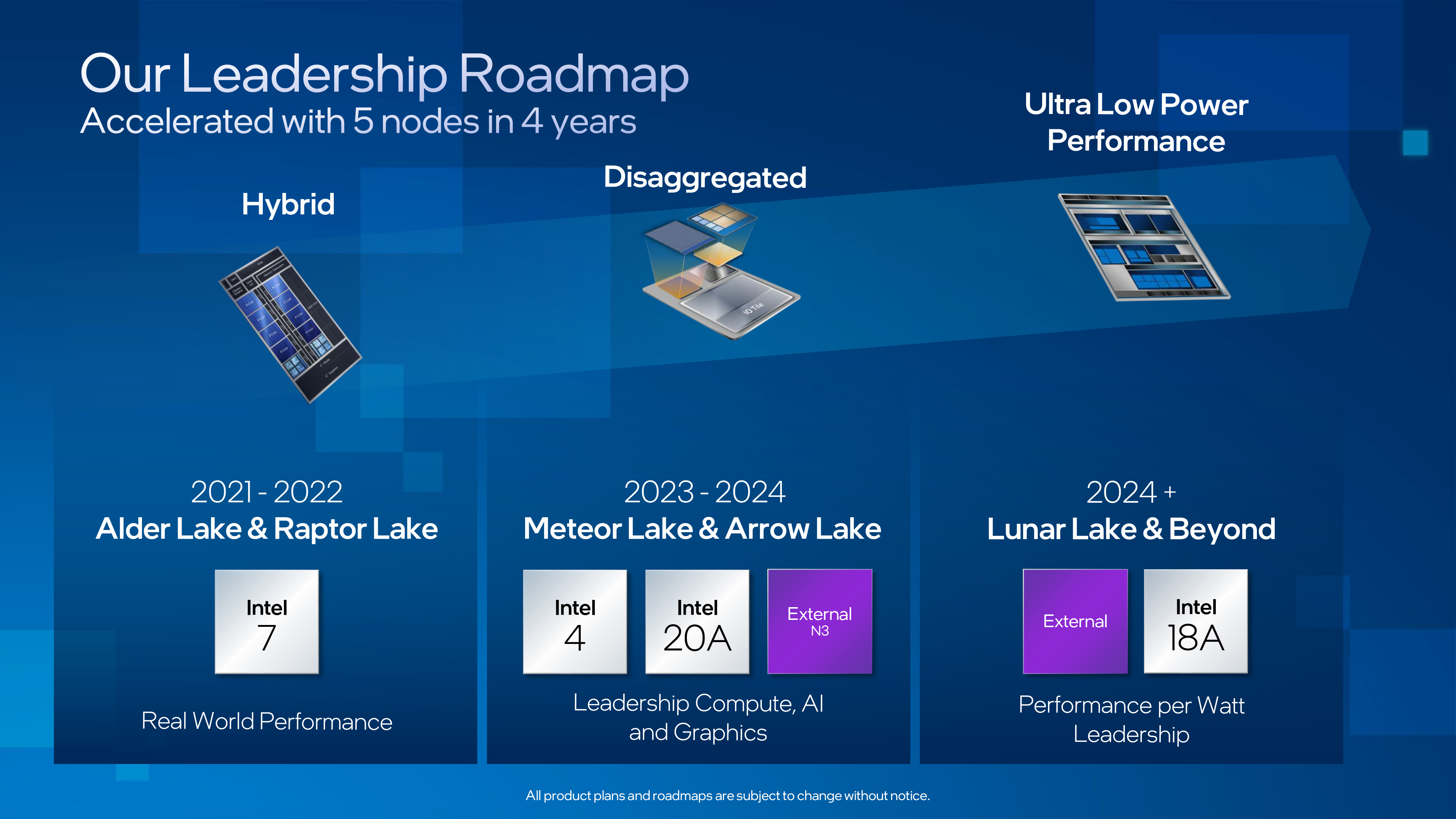
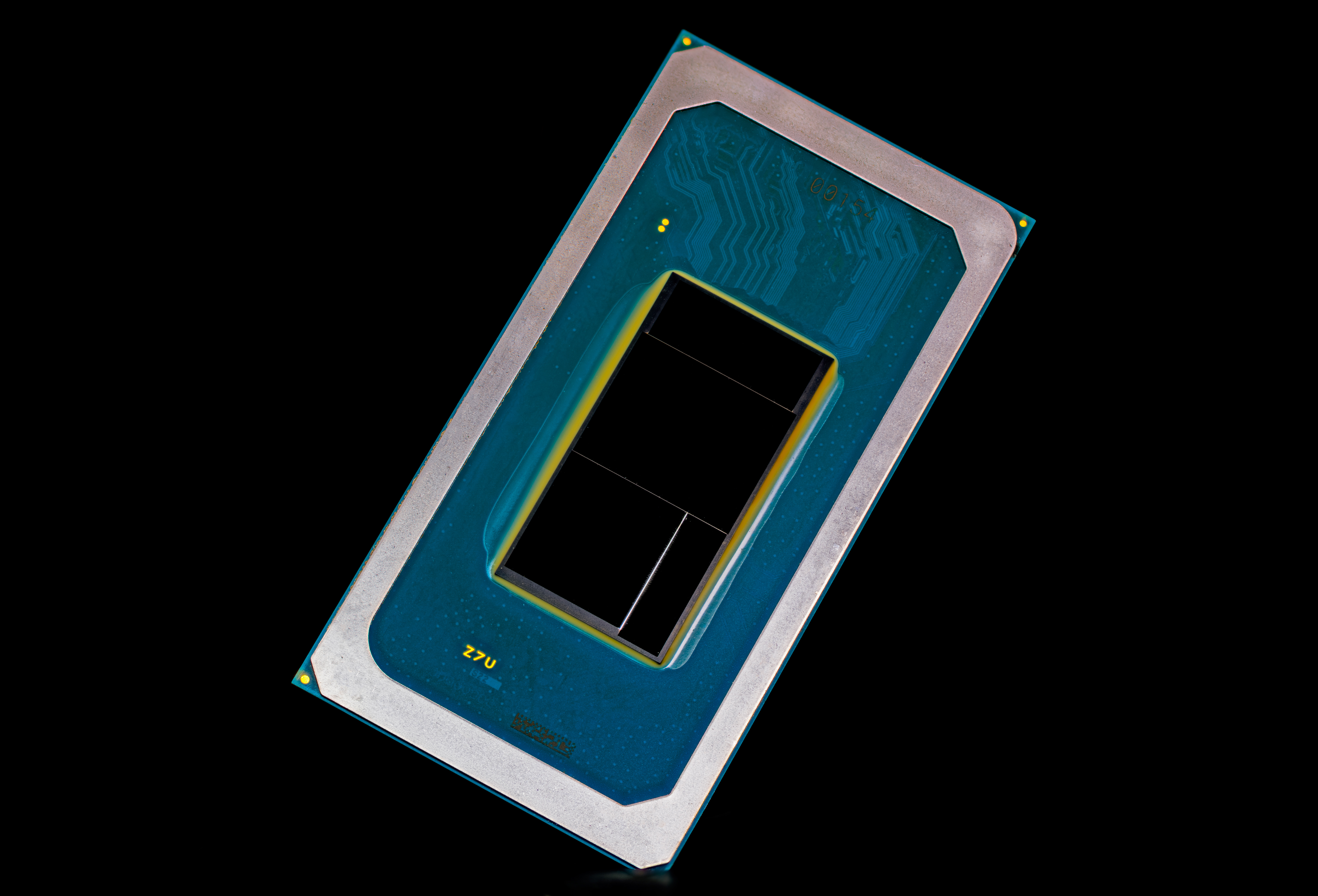
In September, Intel unveiled their chiplet-based Meteor SoC structure throughout their annual Innovation occasion, which slices issues up from a standard monolithic processor into 4 particular person tiles. Created utilizing their Foveros 3D packaging, Intel is utilizing a mixture of course of nodes to place collectively their first chiplet-based CPU. Probably the most vital chiplet, the CPU tile, is being constructed on Intel’s EUV-based Intel 4 node, the newest and best fab tech out of the corporate, and which guarantees to offer sturdy beneficial properties in efficiency and power effectivity in comparison with the long-standing Intel 7 course of. Becoming a member of the CPU tile are tiles for the built-in GPU, SoC, and I/O capabilities, that are constructed on a mixture of trailing-edge and even exterior course of nodes.
Under is our deep dive into Meteor Lake as an SoC structure, in addition to all the important thing elements such because the compute, I/O, graphics, and SoC tile:
Rapidly recapping the Meteor Lake SoC structure, it’s primarily 4 interconnected tiles, together with a compute, graphics, SoC, and an I/O tile. Inside every of the tiles are a bunch of recent developments, together with the Redwood Cove Efficiency (P) cores and Crestmont Effectivity (E) cores housed inside the compute tile. On high of this, Intel additionally has a particular variant of the E-core, known as the Low Energy Island or LP-E core, which is built-in into the SoC tile and is designed to sort out low-intensity workloads. Notably, as a result of the SoC tile is basically all the time energetic, the LP-E core could be very low-cost to make use of from an power standpoint in comparison with powering up the CPU tile.
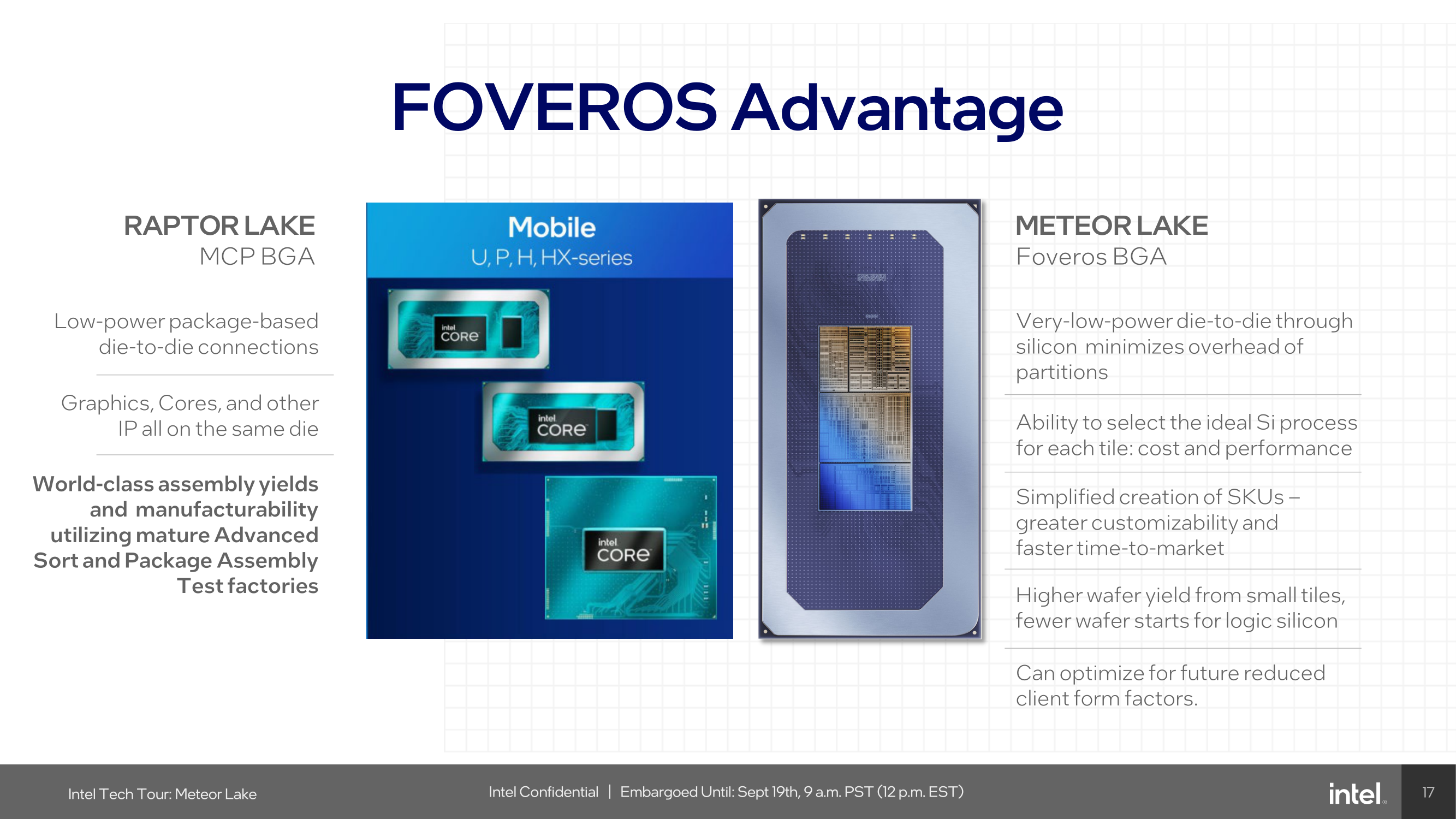
Meteor Lake is an improve and a major architectural shift for Intel, transferring away from conventional monolithic designs to a chiplet-based strategy. This shift, leveraging Intel’s Foveros 3D packaging expertise, introduces 3D chip stacking to beat the constraints of 2D chip layouts. Like different shifts we have seen in direction of utilizing chiplets, the structure’s deal with disaggregation, energy effectivity, and versatile silicon offers Intel new choices for assembling CPUs out of particular person blocks.
The structure’s modular design facilitates scalable energy administration, which will be optimized, permitting every tile to function independently, thereby maximizing efficiency and power effectivity. This disaggregation additionally permits Intel to make use of totally different silicon processes for every tile, providing flexibility and price financial savings in manufacturing. Meteor Lake’s use of Foveros packaging and low-power, low-distance die-to-die interconnects marks a departure from the Multi-Chip Packaging (MCP) used within the earlier Raptor Lake cellular chips, permitting for extra optimized energy utilization and chip customization.
Providing 4 in a different way constructed but extremely practical tiles, Intel’s Meteor Lake seems to be to extend customizations of their pocket book SKUs sooner or later. Providing a tile answer permits Intel to amalgamate a wide range of totally different engines, blocks, and tiles into one chip. Utilizing their Foveros packaging expertise additionally permits Intel to construct chips in a different way, and extra importantly, it means they are not restricted to at least one particular manufacturing course of – a hedge towards issues with anyone fab/node. Even within the current Core Extremely U and H sequence chips Intel is saying in the present day, the manufacturing alternative for every of the tiles differs barely, with the compute tile constructed on Intel 4 node, the graphics tile with Arc Xe graphics is constructed on TSMC’s N5 node, and the SoC and I/O tiles are constructed utilizing TSMC’s N6 course of. This flexibility means Intel can implement new applied sciences from totally different course of nodes, tapping the advantages of any given node’s specialty (e.g. frequency or density) and never having to supply (and yield) a complete chip on a modern course of.
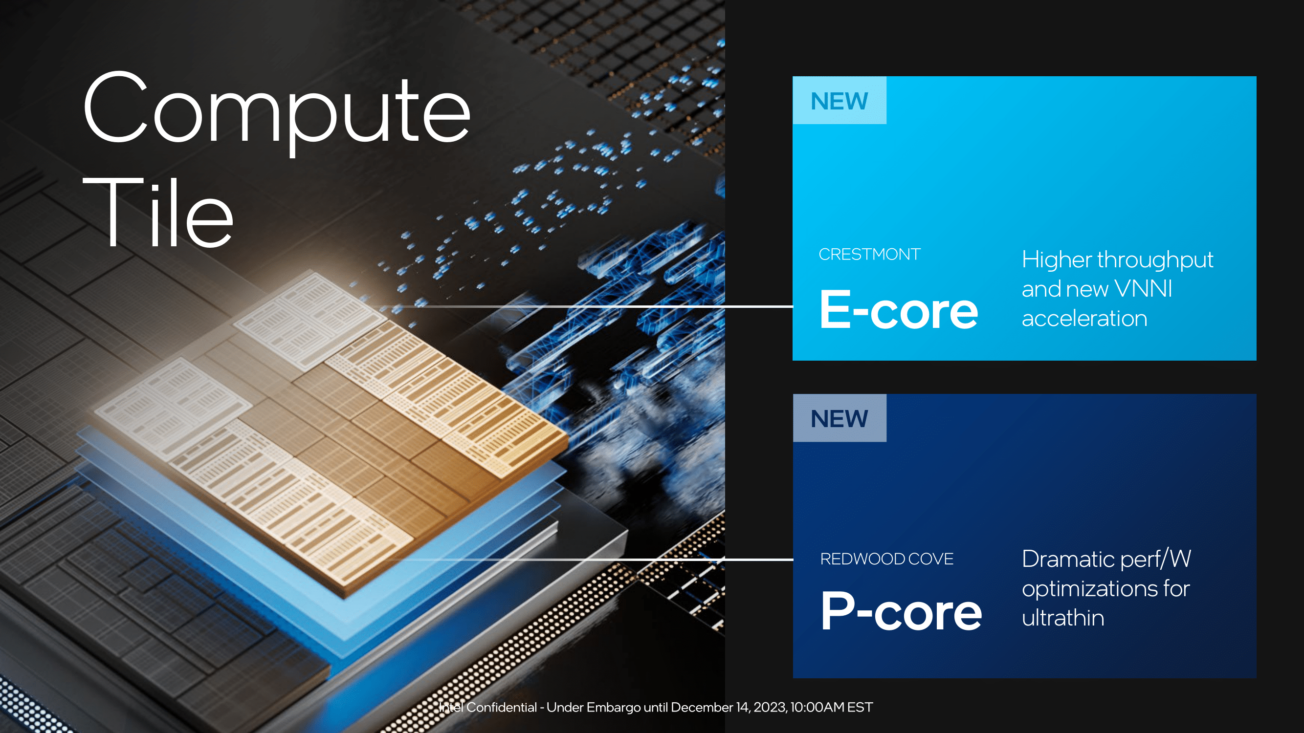
Taking a fast take a look at the underlying structure, on the compute tile of the Extremely Core sequence within the first iteration of Meteor Lake, Intel is utilizing two new CPU architectures inside the heterogeneous design. Intel’s Meteor Lake compute tile is constructed utilizing the Intel 4 node, and the method presents 2x the realm scaling for the high-performance logic libraries in comparison with the earlier Intel 7 node. The most recent Efficiency cores are known as Redwood Cove, which Intel claims brings new advantages over the earlier Golden Cove P-core, together with higher per-watt efficiency effectivity, improved suggestions by Intel Thread Director inside Home windows 11, extra bandwidth, and improved efficiency monitoring capabilities. All of those enhancements mixed are designed to offer enhanced suggestions to Thread Director to assist optimize core efficiency and direct workloads to the best cores.
Notably, nonetheless, Intel hasn’t mentioned something about Redwood Cove’s IPC. Studying between the strains, we’re left with the distinct impression that Redwood Cove’s IPC is analogous (if not similar to) Golden Cove’s. And if that is the case, it means Intel will not be transferring the needle on single threaded efficiency on this technology – no less than, not in TDP-unconstrained situations. In truth, the height P-core clockspeeds for Core Extremely (Meteor Lake) chips are decrease than thirteenth Gen Core Cell (Raptor Lake) chips – 5.1GHz vs. 5.4GHz – so it is totally believable that some Core Extremely chips might lose in single-threaded CPU benchmarks to thirteenth Gen Core chips. All of which is to say that whereas Intel ought to nonetheless decide up some real-world efficiency right here because of the power effectivity enhancements, Redwood Cove is extra of a side-grade when it comes to structure.
Intel’s effectivity cores, however, ought to ship a serious enchancment. Intel is utilizing their Crestmont cores for the effectivity cores, which Intel claims carry IPC beneficial properties over their thirteenth Gen Raptor Lake E-cores, in addition to AI acceleration optimizations in VNNI and ISA, in addition to enhanced suggestions to Intel Thread Director. For low-intensive workloads, Intel consists of two new Low Energy Island (LP-E) cores on every of the introduced SKUs housed inside the SoC tile and permits mild workloads to be offloaded onto these cores to reinforce total energy effectivity. Intel Thread Director with Home windows 11 is a key element in making certain the best workloads go onto the best cores for one of the best efficiency and energy effectivity ranges.
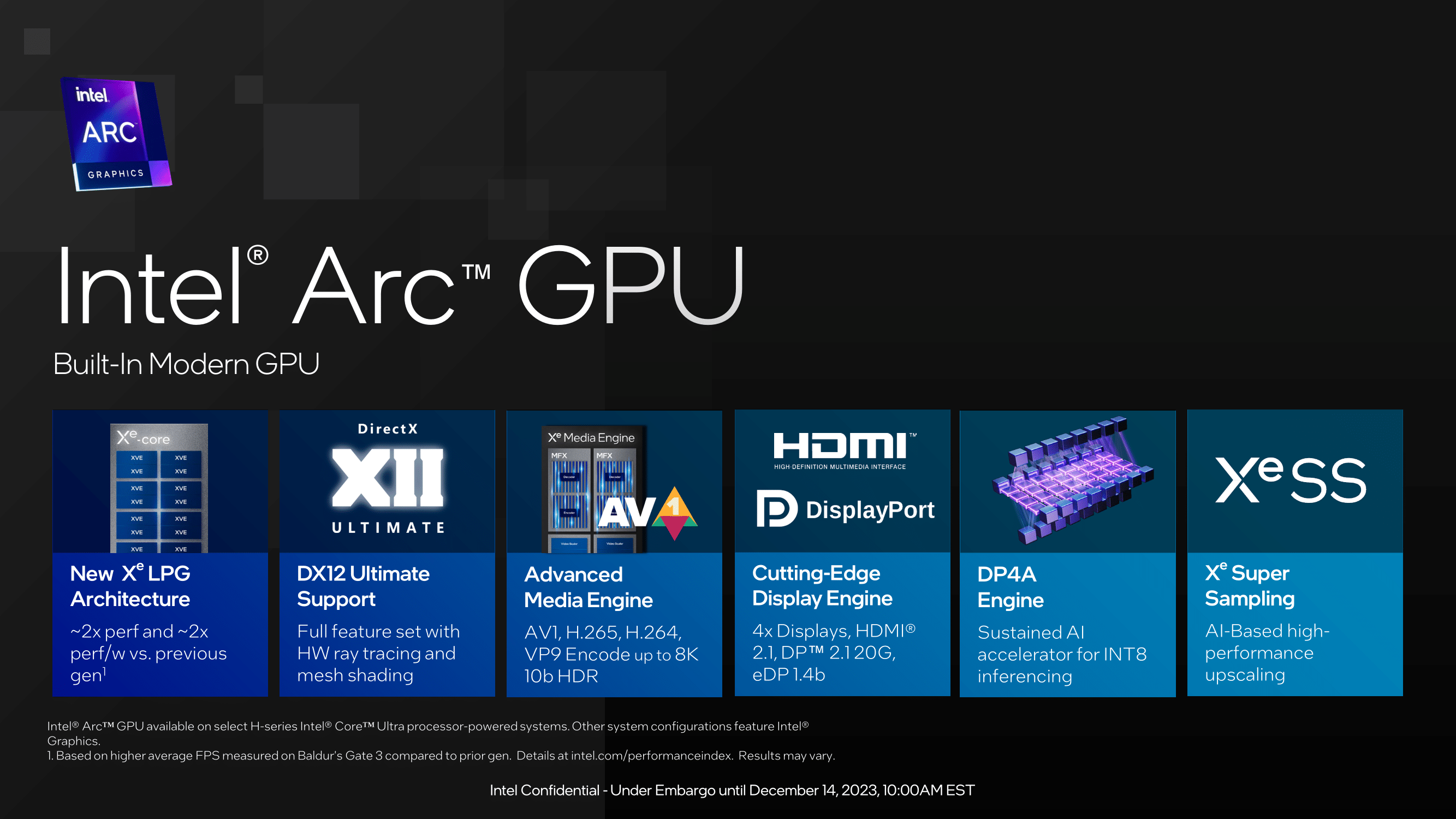
One other key element (or tile) inside the heterogeneous Meteor Lake SoC design is an improve to Intel’s Arc graphics structure. Constructed on TSMC’s N5 node, the graphics core of alternative is the Arc Xe-LPG core, which is a by-product of Intel’s discrete Xe-HPG GPU structure. The GPU tile is comprised of 16 Vector Engines with a 256-bit bus width and 192 KB of shared L1 cache per core. Every Vector Engine can carry out 16 FP32 and 32 FP16 operations per clock, together with a shared FP64 execution port able to 64 INT8 operations per clock. Additionally featured is a devoted FP64 unit, which is new in comparison with Raptor Lake (thirteenth Gen) and has pairs of vector engines working in lockstep for improved effectivity. Notably, this structure doesn’t embody Intel’s matrix engines (XMX), so whereas Intel can run AI duties on the GPU, it would not have fairly the identical punch as on their desktop {hardware}.
For Meteor Lake, Intel has opted to disaggregate the Xe Media Engine from the graphics tile and implanted it inside the SoC tile, which is constructed on TSMC’s N6 node. The Xe Media Engine consists of two multi-format codecs (MFX), that are designed to encode and decode however achieve this off of the GPU to enhance energy effectivity. Meteor Lake helps all kinds of codecs, together with AV1, HEVC, AVC, and VP9, with capabilities together with as much as 8K60 HDR decoding. The Xe Media Engine can also be geared up to deal with as much as 8K 10-bit and HDR encoding.
Launching Softly: Restricted {Hardware} and No Evaluations
Regardless of in the present day being the official launch of the Core Extremely sequence and Meteor Lake platform, you gained’t discover any critiques for the {hardware}. And we’re undecided you’ll be capable of discover a lot {hardware}, both.
In a major departure from how Intel has dealt with earlier mobile-first structure launches, the corporate has not sampled any laptops to the press for evaluate forward of in the present day’s launch. So whilst you can exit and purchase a Core Extremely laptop computer in the present day (in principle, no less than), we are able to’t truly present you the way it performs, and even validate Intel’s personal efficiency claims.
Wanting on the larger image, there are a number of indicators that Intel is struggling to get Meteor Lake out the door for a 2023 launch, which they’ve lengthy promised because it was added to their public roadmap in 2021. The corporate continues to be making an attempt to get better from their a number of fab delays within the 10nm/7nm period, and the chip delays that got here with that. Meteor Lake is Intel’s first main shopper processor constructed with an EUV course of (Intel 4), and delivering it on time could be an vital signal that Intel has put their fab and chip improvement processes again on observe.
Nonetheless, the dearth of evaluate {hardware}, mixed with the truth that the flagship Core Extremely 9 185H SKU gained’t even be out there till Q1, offers us pause. If Meteor Lake is certainly launching in 2023, then it’s solely by the pores and skin of Intel’s enamel: 2 weeks earlier than the top of the 12 months, and what we strongly suspect can be a really restricted variety of laptops out there at retail for in the present day’s launch.
Which isn’t to kick Intel whereas they’re nonetheless making an attempt to select themselves again up. But when Intel hadn’t already promised a 2023 launch for Meteor Lake, then this could virtually definitely would have been a CES launch, if not later.
Within the meantime, all we are able to do for now could be speak about specs and efficiency expectations. Whether or not or not Meteor Lake technically launches in 2023, it’s going to be a 2024 product, and that goes for all the things from critiques to huge {hardware} availability.
The Intel Core Extremely H-Collection: As much as 115 W of Cell Efficiency for Notebooks
With the launch of Intel’s Core Extremely H and U-series, these are the primary chips to function Intel’s new processor branding. As a part of probably the most important model change from Intel within the final 15 years, the Core Extremely 9, 7, and 5 sequence is designed to separate their shopper chips into simply denote classes, with the Extremely naming reserved for his or her premium components. The most important change is that Intel is dropping the ‘i’ prefix, which is probably one in all their most denominable processor identities during the last 15 years, e.g., the Core i5.
Intel is launching 4 SKUs below their Core Extremely branding for the H-series, overlaying the Extremely 7 and Extremely 5 segments. The flagship Extremely 9 chips, however, will stay lacking in motion for one more quarter – the Core Extremely 9185H is not anticipated to launch till someday in Q1 2024. It is value highlighting Intel’s message right here, which appears to be combined. Usually, the U-series SKUs are reserved for ultrathin notebooks and ultraportables, whereas Intel’s message seems to be to spotlight that the H-series might be utilized in thinner notebooks too. This stays to be seen, and we’ll discover out quickly sufficient when OEMs and distributors begin saying fashions encompassing Meteor Lake.
Opening with a glance and dissection of the specs on the chips out there now, the Core Extremely 7 165H and Core Extremely 7 155H are 16C/22T components. With six efficiency (P) cores and eight effectivity (E) cores, including within the two LP-E cores on the SoC tile brings us to a complete of 16 CPU cores that may execute as much as 22 threads directly. The Core Extremely 7 165H has a P-core turbo frequency of as much as 5.0 GHz with an E-core turbo frequency of as much as 3.8 GHz. This additionally consists of 8 Intel Arc Xe cores for the built-in graphics, which may hit to 2.3 GHz and 24 MB of Intel Good L3 cache.
The Intel Core Extremely 7 155H is barely slower than the Core Extremely 7 165H, with a 5.0 GHz P-Core turbo and a 2.25 GHz built-in graphics frequency. The brand new Crestmont E-cores can hit a most of three.8 GHz, whereas the Core Extremely 7 155H additionally has 24 MB of L3 cache. The one distinction between the 2 Core Extremely 7 SKUs is a 100 MHz dip within the P-core turbo and a slight 50 MHz dip in graphics clock velocity.
Each chips function with a reasonably huge TDP vary. The bottom TDP of the Extremely 7 (and Extremely 5) H-series components is simply 28 Watts, whereas your entire lineup can turbo at both 64 Watts, or for the quickest units, 115 Watts. And since we’re speaking about cellular components, do needless to say system distributors have lots of latitude right here for additional adjusting TDP limits to suit the facility and cooling constraints of their units.
It is value highlighting that Intel is evaluating lots of the Core Extremely H-series up towards the earlier thirteenth Gen Raptor Lake-Based mostly P-SKUs (28/64 W) in terms of efficiency, reasonably than the the 13th Gen H-series parts. Coming from the earlier generations, the bottom TDP for the H-series has been decreased, from 45 W down to twenty-eight W. In apply, Intel has seemingly collapsed the P and H sequence (which had been already utilizing the identical silicon and packages) all the way down to a single line, the H-series, for the primary technology of Core Extremely.
| Intel Core Extremely H-Collection Processors: Meteor Lake (Intel 4) | ||||||||
| AnandTech | Cores (P+E+LP/T) |
P-Core Turbo Freq |
E-Core Turbo Freq |
GPU | GPU Freq | L3 Cache (MB) |
Base TDP | Turbo TDP |
| Extremely 9 | ||||||||
| Core Extremely 9 185H* | 6+8+2/22 | 5100 | 3800 | Arc Xe (8) | 2350 | 24 | 45 W | 115 W |
| Extremely 7 | ||||||||
| Core Extremely 7 165H | 6+8+2/22 | 5000 | 3800 | Arc Xe (8) |
2300 | 24 | 28 W | 64/115 W |
| Core Extremely 7 155H | 6+8+2/22 | 4800 | 3800 | Arc (8) | 2250 | 24 | 28 W | 64/115 W |
| Extremely 5 | ||||||||
| Core Extremely 5 135H | 4+8+2/18 | 4600 | 3600 | Arc Xe (7) |
2200 | 18 | 28 W | 64/115 W |
| Core Extremely 5 125H | 4+8+2/18 | 4500 | 3600 | Arc Xe (7) | 2200 | 18 | 28 W | 64/115 W |
*Accessible from Q1 2024
Be aware: Intel hasn’t supplied us with any base frequency specs on the time of writing, as soon as now we have these, we’ll replace the tables.
Shifting all the way down to the Core Extremely 5 sequence SKUs, just like the Core Extremely 7 H-series, there are minor variations within the specs. The sooner of the 2, albeit with a 100 MHz sooner P-core turbo, is the Core Extremely 5 135H, which is a 14C/18T chip, with 4 P-cores and eight E-cores making up the compute tile on the 2 Core Extremely 5 components. The Core Extremely 5 135H has a 4.6 GHz P-Core turbo with a 3.6 GHz E-core turbo, though there’s a barely decrease spec Intel Arc graphics tile with 7 Xe graphics cores that may hit as much as 2.2 GHz.
The Core Extremely 5 125H has a 4.5 GHz P-Core turbo, the identical 3.6 GHz E-core turbo because the 5 135H, and shares the identical Arc built-in graphics clocked as much as 2.2 GHz. Each the Intel Core Extremely 5 135H and Core Extremely 5 125H have a base TDP of 28 W, though Intel has supplied each a 64 or 115 W turbo TDP specification.
The final of the introduced Intel Core Extremely H-series SKUs coincidentally has the very best specs, nevertheless it will not be out there till Q1 2024, which is the Core Extremely 9 185H. Like the 2 Core Extremely 7 chips introduced, the Core Extremely 9185 can also be a 6P+8E+2LP/22T chip with P-Core turbo clock speeds of as much as 5.1 GHz and an E-Core turbo frequency of three.8 GHz. It has the identical Arc-based 8 Xe cores inside the graphics tile and is clocked as much as 2350 MHz. Not like the opposite Core Extremely H-series processors, the Core Extremely 9185 has a better 45 W base TDP, with a 115 W most TDP at turbo clock speeds.
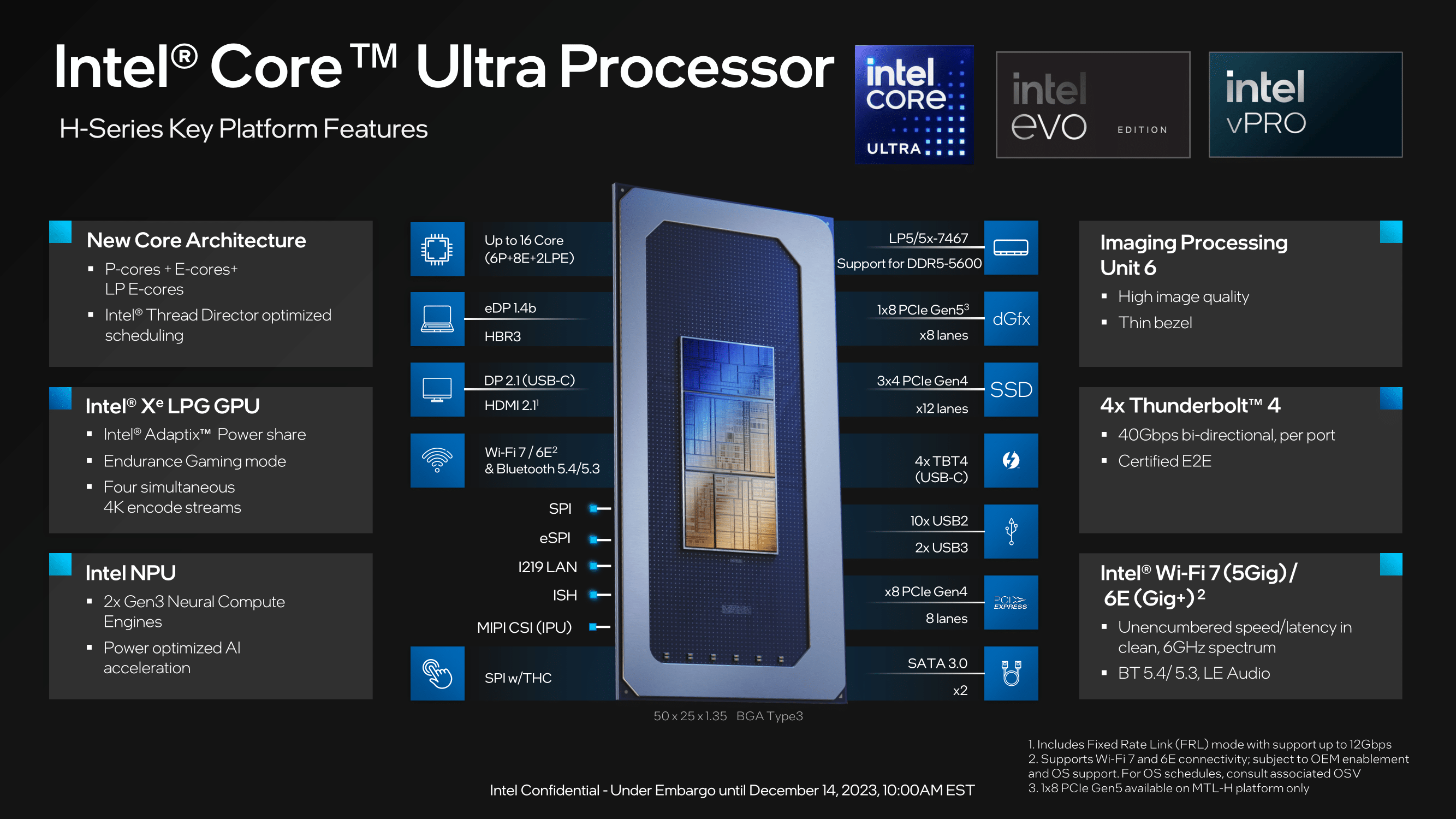
The entire Intel Core Extremely H sequence SKUs embody the aforementioned 2 Low Energy Island (LP-E) cores constructed instantly into the SoC tile. They’re designed to enhance energy effectivity by placing low-intensity workloads on the extra environment friendly of the three out there core varieties. Additionally current inside the SoC tile are two Neural Compute Engines, that are Intel’s implementation of an NPU designed for generative AI and are optimized for most of these workloads.
In the meantime, reminiscence help for the Core Extremely H-series platform consists of each DDR5 and LPDDR5(X). The processor is at present validated towards DDR5-5600 and LPDDR5X-7467, all hooked up through a 128-bit reminiscence bus.
For inside I/O, Intel is providing a mixture of PCIe 5.0 and PCIe 4.0 lanes on the Core Extremely H-series platform. A single PCIe 5.0 x8 hyperlink is out there for OEMs seeking to embody discrete graphics inside their fashions. In the meantime there are 12 PCIe 4.0 lanes devoted to driving storage, supporting as much as three PCIe 4.0 x4 M.2 SSDs. Lastly, one other 8 PCIe 4.0 lanes can be found for common I/O wants. And for programs that also want further storage past that – significantly of the rotating rust selection, there are a pair of SATA III ports out there on the chip.
As for exterior I/O, the Core Extremely H-series platform consists of help for 4x Thunderbolt 4 (USB4) ports, in addition to 2x USB 3 and 10x USB 2 ports. The built-in GPU, in flip, can drive DisplayPort 2.1 video out through the Sort-C ports, and the silicon helps a devoted HDMI 2.1 port if an OEM desires to incorporate one.
Lastly, on the wi-fi facet of issues, the Meteor Lake platform natively helps Wi-Fi 6E. That is achieved through the newest technology of Intel’s CNVio expertise, which integrates a Wi-Fi MAC in to the host chipset (or this case, the SoC), whereas the PHY stays a separate module. Integrating it on this style retains down prices (OEMs want solely purchase the PHY) and makes for a smaller footprint total.
Intel can also be itemizing Wi-Fi 7 help for Meteor Lake, nevertheless it must be famous that that is wholly discrete; there is no such thing as a native Wi-Fi 7 {hardware} inside the Meteor Lake platform itself OEMs seeking to incorporate Wi-Fi 7 would wish to incorporate a stand-alone adapter, corresponding to Intel’s BE200. Consequently, we’re anticipating to see Wi-Fi 7 help restricted to premium notebooks, the place OEMs can cross on the upper price of a discrete adapter and have the area to position it.
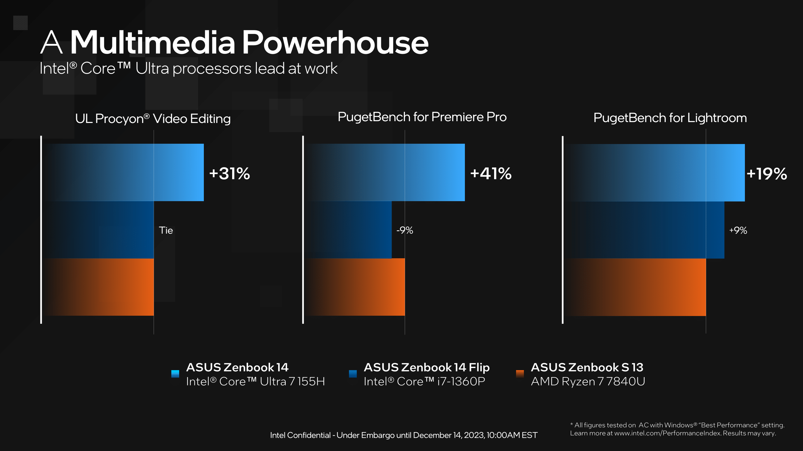
Taking a look at among the efficiency figures Intel supplied inside their Core Extremely sequence slide deck, Intel is claiming a efficiency achieve of as much as 31% inside UL Procyon’s video modifying benchmark, with a fair bigger achieve of 41% over the AMD Ryzen 7 7840U processor in PugetBench for Premiere Professional. Utilizing PugetBench for Lightroom, Intel claims the Core Extremely 7 115H is nineteen% sooner on this state of affairs. Whereas we take vendor and producer’s in-house efficiency figures with a grain of salt, they nonetheless point out anticipated efficiency from new merchandise.
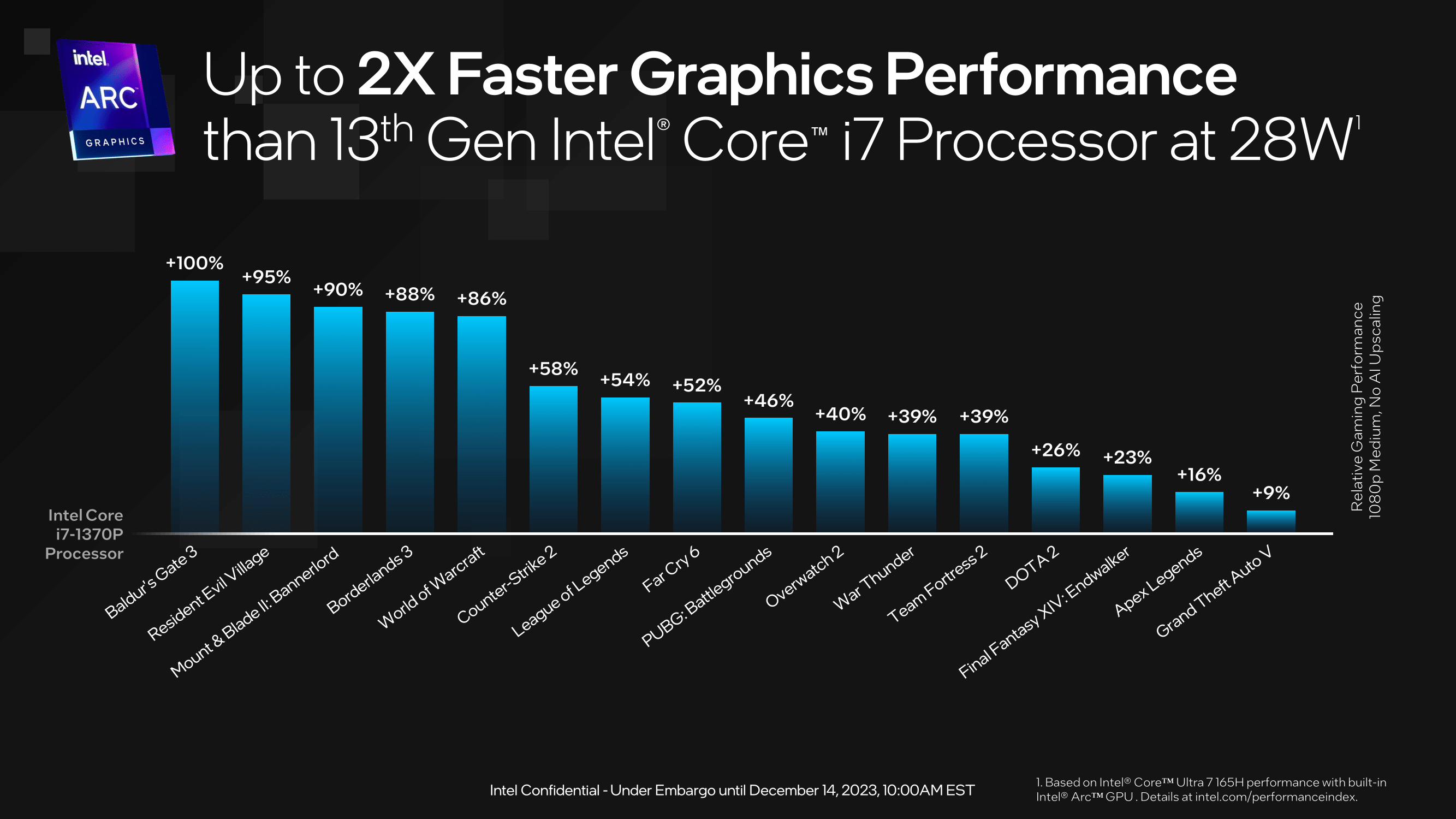
As for GPU performnace, Intel is evaluating the newest Arc Xe-LPG built-in graphics on the Core Extremely 7 165H for gaming efficiency to the earlier technology Core i7-1370P. From the in-house testing Intel did, they declare as much as 100% beneficial properties in Baldur’s Gate 3, with various ranges of efficiency in different video games, corresponding to 88% extra FPS in World of Warcraft and 39% in Crew Fortress 2. Whereas it is clear that Intel is pinning lots of Meteor Lake efficiency success on the Arc-based built-in graphics, it is going to be attention-grabbing to see how the efficiency stacks up towards discrete choices within the coming months.
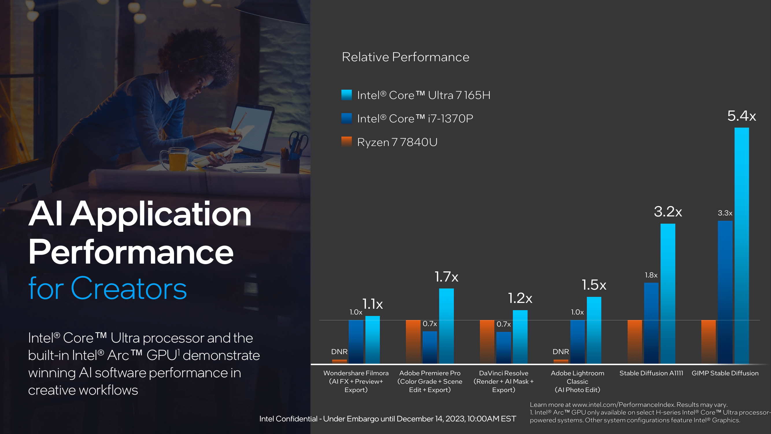
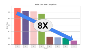
The opposite metric the place Intel is seeking to showcase their benefit over the competitors is in AI efficiency. Intel is claiming as much as 5.4 X efficiency in GIMP Secure Diffusion with simply the improved capabilities from inside the Arc Xe-LPG graphics cores over the earlier Core i7-1370P and AMD Ryzen 7 7840U processor. Even in functions using generative AI corresponding to Adobe Lightroom, Intel claims as much as 1.5 X the efficiency of the Ryzen 7 7840U.
Once more, take vendor/OEM-supplied efficiency figures with a grain of salt. Nonetheless, the efficiency beneficial properties Intel is displaying for the Core Extremely H sequence look spectacular on paper, however experiences and figures in the true world might differ.
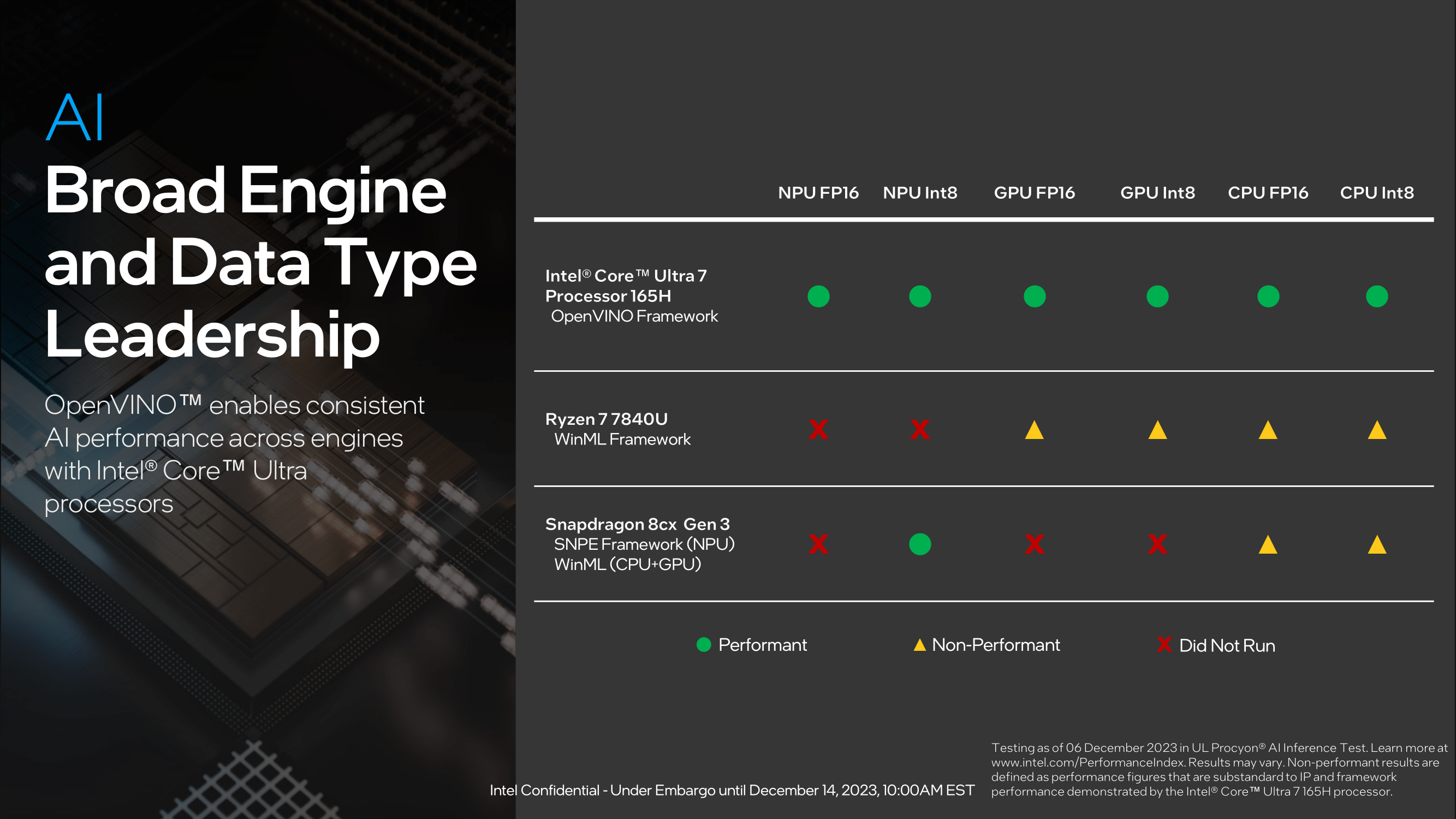
Intel’s Meteor Lake SoC combines a practical and multi-dimensional strategy to AI inferencing, with generative AI throughout the compute, graphics, and NPU engine block. Intel is creating a transparent image that Meteor Lake has three totally practical AI engines, with the Arc Xe-LPG graphics offering excessive throughput for AI acceleration for content material creation. In distinction, the NPU and its two Neural Compute Engines are designed to dump sustained AI workloads to additional improve energy effectivity. The Compute tile itself and the mixture of the Redwood Cove (P) and Crestmont (E) cores are designed to deal with AI workloads with a decrease latency for extra precision.
With the PC CPU ecosystem now in a full-on dash to combine improved AI/neural community talents into their designs, we’re additionally going to see lots of back-and-forth between distributors on their NPU capabilities and efficiency in these early days. The most recent and most up-to-date half to launch, Intel is fast to tout its help for a big array of numerical codecs. Serving to issues in Intel’s case, the corporate is coming into this launch with their already well-developed OpenVINO framework to faucet the mixed CPU, GPU, and NPU AI capabilities of their {hardware}.
Intel’s in-house testing within the above chart ran the UL Procyon AI inference benchmark, which is a little bit of a messy comparability because of the benchmark’s help for various and vendor-specific backends. Once more, experiences and efficiency might differ.
Intel Core Extremely U-Collection: Decrease TDPs for Even Thinner and Low Profile Notebooks
Shifting onto the brand new Intel Core Extremely U-series processors, Intel has readied 4 SKUs out there now, whereas one other two are set to be out there someday in Q1 2024.
Beginning issues off, now we have the Intel Core Extremely 7 165U, a 2P+8E+2LP/14T chip with a P-core turbo of as much as 4.9 GHz and an E-core turbo frequency of three.8 GHz. The 7 165U additionally has 4 Xe built-in graphics cores clocked at 2.0 GHz. The one distinction between the Core Extremely 7 165U and the Core Extremely 7 155U is that the 7 155U is barely slower with a 4.8 GHz P-Core turbo (100 MHz decrease) and a 1.95 GHz clocked built-in graphics (50 MHz decrease).
| Intel Core Extremely U-Collection Processors: Meteor Lake (Intel 4) | ||||||||
| AnandTech | Cores (P+E+LP/T) |
P-Core Turbo Freq |
E-Core Turbo Freq |
GPU | GPU Freq | L3 Cache (MB) |
Base TDP | Turbo TDP |
| Extremely 7 | ||||||||
| Core Extremely 7 165U | 2+8+2/14 | 4900 | 3800 | Arc Xe (4) | 2000 | 12 | 15 W | 57 W |
| Core Extremely 7 164U* | 2+8+2/14 | 4800 | 3800 | Arc Xe (4) | 1800 | 12 | 9 W | 30 W |
| Core Extremely 7 155U | 2+8+2/14 | 4800 | 3800 | Arc Xe (4) | 1950 | 12 | 15 W | 57 W |
| Extremely 5 | ||||||||
| Core Extremely 5 135U | 2+8+2/14 | 4400 | 3600 | Arc Xe (4) | 1900 | 12 | 15 W | 57 W |
| Core Extremely 5 134U* | 2+8+2/14 | 4400 | 3800 | Arc Xe (4) | 1750 | 12 | 9 W | 30 W |
| Core Extremely 5 125U | 2+8+2/14 | 4300 | 3600 | Arc Xe (4) | 1850 | 12 | 15 W | 57 W |
*Accessible from Q1 2024
The Intel Core Extremely 5 (U) sequence lineup is comprised of three SKUs, two of which can be found in the present day and one (Core Extremely 5 134U) that’s set to launch in Q1 2024. Beginning with the Core Extremely 5 135U, it has a CPU core configuration of 2P+8E+2LP/14T, a P-core turbo of as much as 4.4 GHz, and an E-core turbo of as much as 3.6 GHz. For the built-in graphics, the graphics tile has 4 Arc Xe graphics cores clocked at 1.9 GHz, and like the remainder of the U-series chips, it has 12 MB of L3 cache. The Core Extremely 5 125U has the identical 2P+8E+2LP/12 core configuration, with a 4.3 GHz P-core turbo and a 50 MHz slower built-in graphics frequency of 1.85 GHz.
The entire Core Extremely U-series processors introduced in the present day function a 2P+8E configured compute tile, with 4 Xe Arc built-in graphics cores, 12 MB of L3 cache, and include a base TDP of 15 W and a turbo TDP of 57 W. Very like the Core Extremely H-series, the Core Extremely U-series additionally embody 2 LP-E cores inside the SoC tile, in addition to 2 Neural Compute Engine cores designed to sort out AI inferencing and generative AI workloads.
And whereas not depicted in any of Intel’s diagrams, the U-series chips supply related inside and exterior I/O capabilities because the H-series chips. The most important distinction is that the U-series chips drop the PCIe 5.0 lanes for discrete graphics; in order that leaves the 12 PCie 4.0 lanes for storage, and one other 8 PCIe 4.0 lanes for common I/O. And for exterior I/O, there’s help for 4x Thunderbolt 4 (USB4) ports, in addition to 2x USB 3 and 10x USB 2 ports.
In the meantime, Intel is doing one thing just a little totally different with the 2 Core Extremely U-series chips that can be launching someday in Q1 2024. The most important distinction right here is that they’ve a 9 W base TDP with a turbo TDP of 30 W, round half that of the opposite U-series chips. The Core Extremely 7 164U and the Core Extremely 5 134U are each 2P+8E+2LP/14T chips with the identical turbo clock speeds as the highest sequence counterparts (7 165U and 5 135U) however with decrease Arc graphics frequencies, which sit at 1.8 GHz for the 7 164U and 1.75 GHz for the 5 134U.
Extra attention-grabbing, maybe, is that these chips don’t help DDR5 reminiscence in any respect. As a substitute, solely LPDDR5(X) is supported, and solely at speeds as much as 6400 MT/sec, a bit slower than the LPDDR5X-7467 fee supported by the remainder of the Core Extremely stack. With these 9W SKUs primarily being the successor to the outdated ultra-low-power Y-series chips, it is unsurprising to see that Intel is just supporting extremely power environment friendly reminiscence configurations.
General, these chips are primarily designed for the thinnest and lightest notebooks, which want particularly low-TDP processors to match their cooling talents and battery capacities. That is additionally the place we’ll presumably see Intel’s Type4 chip packaging used (depicted above), as area is at a premium in these designs.
Intel Core Extremely H and U-Collection Availability: Some Accessible Now, Extra Coming Q1 2024
A minimum of for the primary Meteor Lake cellular SKUs, Intel seems to be to be specializing in getting as a lot enhanced generative AI performance into the market as shortly as potential. With 2024 shaping as much as be a pivotal 12 months for consumer-driven AI inferencing, Intel’s Core Extremely sequence seems to be to compete instantly towards AMD’s Ryzen 8040 APU series, which is a complete refresh of their Pheonix silicon however with a wider deal with Ryzen AI; AMD’s interpretation of on-chip AI inferencing.
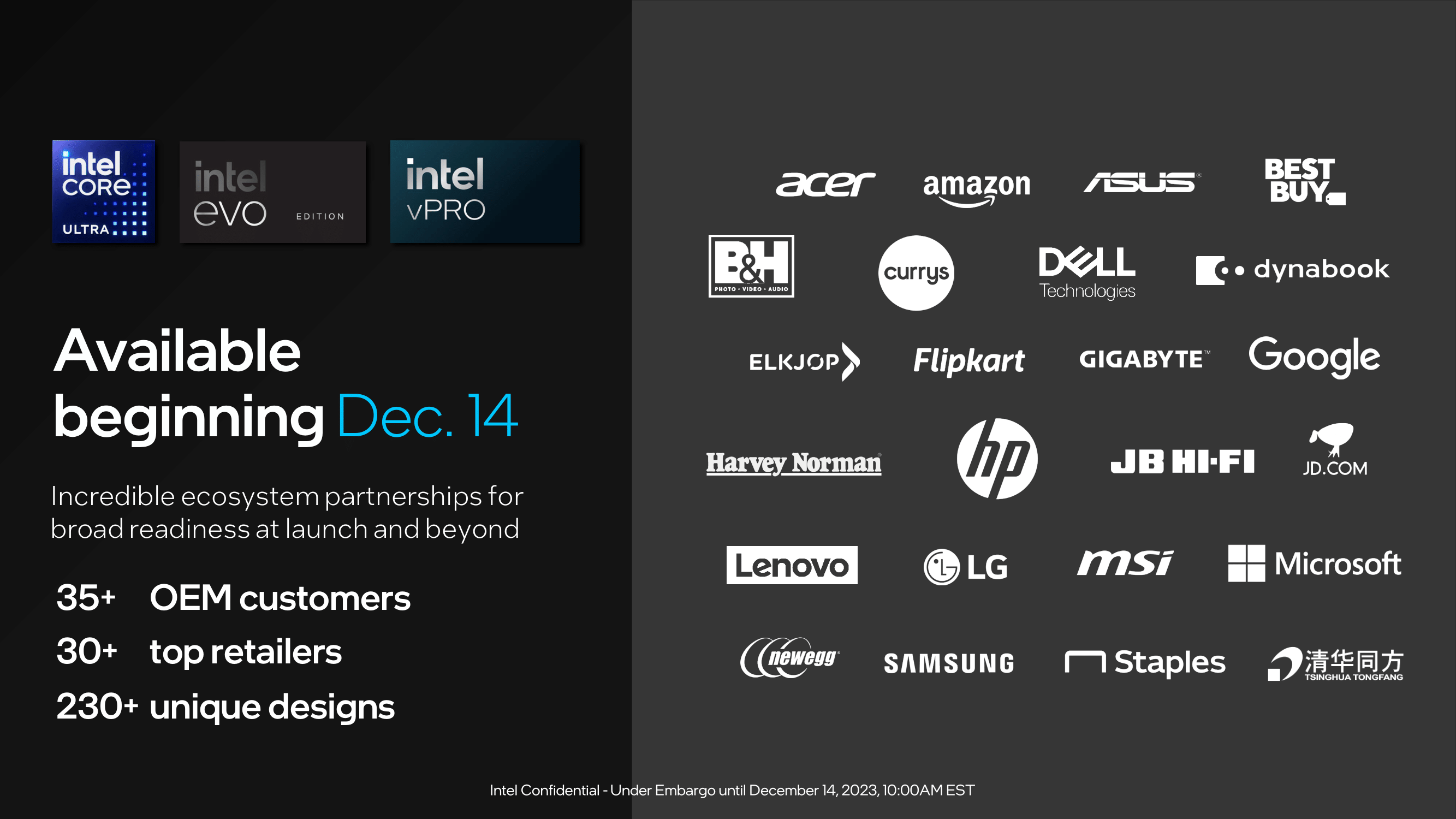
The Intel Core Extremely H and U-series processors can be found in the present day, with over 35 OEMs providing totally different fashions, together with Acer, ASUS, Dell, HP, Lenovo, and MSI. The one SKUs not launching in the present day embody the Intel Core Extremely 9 185H, Core Extremely 7 164U, and Core Extremely 5 134U, that are anticipated to launch someday in Q1 2024. On the time of writing, no OEMs have reached out to us with fashions, and pricing on every half stays unknown.