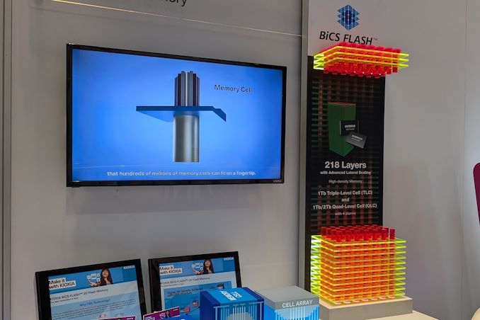
218 Layers With Superior Scaling
Kioxia’s sales space at FMS 2024 was a busy one with a number of know-how demonstrations conserving guests occupied. A walk-through of the BiCS 8 manufacturing course of was the primary to seize my consideration. Kioxia and Western Digital announced the sampling of BiCS 8 in March 2023. We had touched briefly upon its CMOS Bonded Array (CBA) scheme in our protection of Kioxial’s 2Tb QLC NAND device and coverage of Western Digital’s 128 TB QLC enterprise SSD proof-of-concept demonstration. At Kioxia’s sales space, we acquired extra insights.
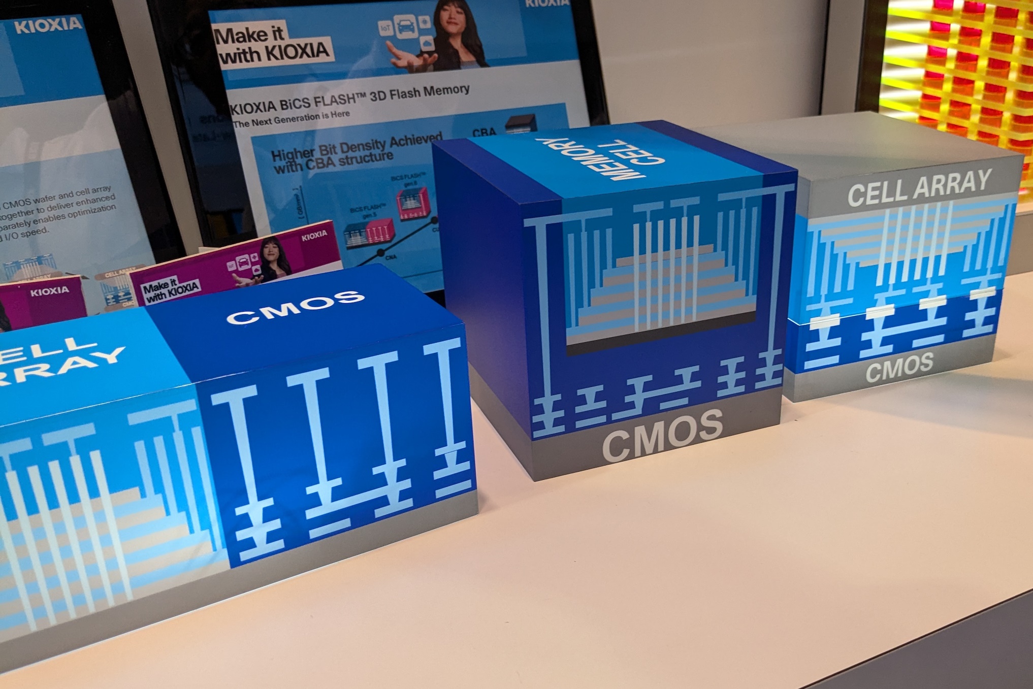
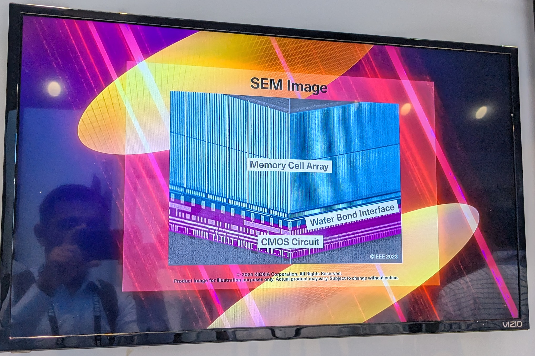
Historically, fabrication of flash chips concerned placement of the affiliate logic circuitry (CMOS course of) across the periphery of the flash array. The method then moved on to placing the CMOS underneath the cell array, however the wafer growth course of was serialized with the CMOS logic getting fabricated first adopted by the cell array on high. Nonetheless, this has some challenges as a result of the cell array requires a high-temperature processing step to make sure greater reliability that may be detrimental to the well being of the CMOS logic. Due to latest developments in wafer bonding strategies, the brand new CBA course of permits the CMOS wafer and cell array wafer to be processed independently in parallel after which pieced collectively, as proven within the fashions above.
The BiCS 8 3D NAND incorporates 218 layers, in comparison with 112 layers in BiCS 5 and 162 layers in BiCS 6. The corporate determined to skip over BiCS 7 (or, somewhat, it was in all probability a short-lived technology meant as an inside take a look at automobile). The technology retains the four-plane cost entice construction of BiCS 6. In its TLC avatar, it’s obtainable as a 1 Tbit gadget. The QLC model is offered in two capacities – 1 Tbit and a couple of Tbit.
Kioxia additionally famous that whereas the variety of layers (218) would not evaluate favorably with the most recent layer counts from the competitors, its lateral scaling / cell shrinkage has enabled it to be aggressive when it comes to bit density in addition to working speeds (3200 MT/s). For reference, the most recent transport NAND from Micron – the G9 – has 276 layers with a bit density in TLC mode of 21 Gbit/mm2, and operates at as much as 3600 MT/s. Nonetheless, its 232L NAND operates solely as much as 2400 MT/s and has a bit density of 14.6 Gbit/mm2.
It should be famous that the CBA hybrid bonding course of has benefits over the present processes utilized by different distributors – together with Micron’s CMOS underneath array (CuA) and SK hynix’s 4D PUC (periphery-under-chip) developed within the late 2010s. It’s anticipated that different NAND distributors may even transfer finally to some variant of the hybrid bonding scheme utilized by Kioxia.