First Chips Booting, First Exterior Buyer Tape-Out in H1’25
Following Intel’s painful Q2 earnings name and the announcement of their 2025 cost reduction plan final week, it has turn out to be more and more evident that Intel’s future is within the arms of their foundry group. Between Intel’s IDM 2.0 initiative and their inside chip manufacturing plans, all roads lead again to Intel retaking – and retaining – fab course of management. To win as each a chip designer and a contract chip maker, Intel wants to have the ability to regain the fab know-how lead it as soon as held. In lots of respects it’s a return to Intel’s traditional (and most profitable) working mannequin, however by no means has it been so dangerous at it’s for the already weakened Intel.
Intel’s do-or-die sprint for course of management signifies that, for the subsequent 18 months or so, all eyes are on the corporate’s 20A and 18A course of nodes. The ultimate nodes of their formidable 5 Nodes in 4 Years roadmap, the twinned 20A/18A are the end result of a number of new applied sciences, primarily Intel’s GAAFET implementation (RibbonFET), which is being mixed with PowerVia, Intel’s bottom energy supply community (BS-PDN) know-how. 20A is about to function Intel’s early model of the node, and 18A the refined model for long-term use each internally, and because the first main exterior node for Intel Foundry. To say that the whole lot rides on Intel 18A isn’t fairly correct, but it surely’s solely a slight embellishment.
To that finish, we’re going to see Intel ship numerous standing updates on 18A over the subsequent yr as they proceed to stipulate to traders and exterior clients alike that they’ve the manufacturing facet of their enterprise so as. And at present is a type of days, with a contemporary replace on the state of 18A.
18A Chips Again & Booting
So what’s new with 18A? The largest information out of Intel this morning is that their first 18A chips are again from the event fab and are efficiently booting working methods. This implies the silicon not solely works (power-on), however works nicely sufficient to finish core duties. It’s a serious step in mentioning a chip, and at this level, Intel needs to verify to let the entire world know.
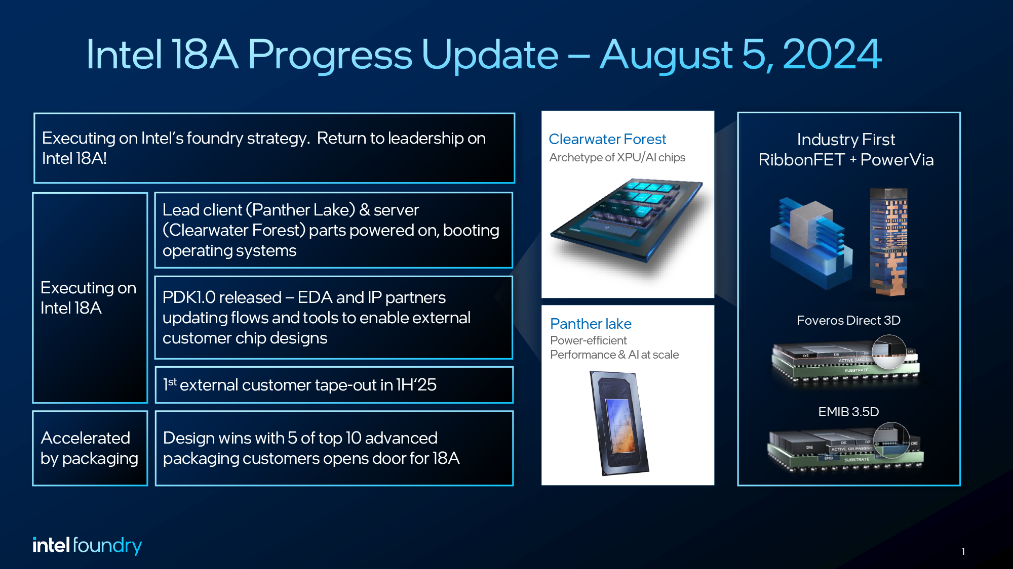
Earlier this yr the corporate completed taping out each of its lead 18A chips: Panther Lake for shoppers, and Clearwater Forest for servers. And it’s each chips which can be booting. That is made all of the extra important by the truth that Clearwater Forest additionally depends on Intel’s die-to-die hybrid bonding packaging know-how, Foveros Direct 3D, the place will probably be the lead product for that know-how as nicely. Which for Intel, is a promising signal that not solely are their silicon lithography ambitions paying off, however their intention to guide in superior packaging is on-track as nicely.
And whereas Intel doesn’t usually speak about yields this early within the recreation, it’s fascinating to notice that in a separate Q&A being revealed this morning with Intel Foundry’s new boss, Kevin O’Buckley, the top of Foundry Providers explicitly feedback that Panther Lake is “yielding nicely”. Equally, Panther Lake’s DDR reminiscence controller (a fancy block mixing logic with a PHY) is already working at its goal frequency. Progress goes so nicely, apparently, that in response to O’Buckley, it’s forward of schedule on its product qualification milestones.
PDK 1.0 Launched, First Exterior Buyer Tape-Out Anticipated in H1’25
As for Intel’s contract foundry enterprise, the corporate is ramping up its efforts there now that the primary full course of design package (PDK) is prepared for 18A. Intel launched their 18A PDK 1.0 final month, giving Intel’s clients (and potential clients) the instruments to lastly end designing their chips for manufacturing. As is often the case of a brand new node, pre-release PDKs had been out there for corporations to get began on their designs, however the 1.0 PDK is often wanted to complete these designs and align them with the formal and finalized course of specs.
For Intel, getting an exterior PDK out for a modern course of node is not any small feat, as the corporate has spent a long time working its fabs for the advantage of its inside product design groups. A helpful PDK for exterior clients – and actually, a helpful fab atmosphere altogether – not solely wants course of nodes that persist with their specs somewhat than making bespoke changes, but it surely signifies that Intel must doc and outline all of this in a helpful, trade normal style. One of many main failings of Intel’s earlier efforts to get into the contract foundry enterprise, in addition to being half-hearted efforts general, is that they didn’t creator PDKs that exterior corporations may simply use. On the finish of the day, Intel is trying to woo clients from TSMC and Samsung, and as such Intel wants to supply PDKs that chip designers accustomed to modern contract fabs can use.
These efforts are lastly paying off, if slowly. Whereas nonetheless not sharing any names, Intel expects their first exterior buyer chip design will tape out within the first half of 2025 (H1’25). And, as Intel hopes, will probably be the primary of many.
In the end, the arduous work for Intel foundry will not be but full, and it’ll proceed from right here. With preliminary 18A growth wrapping up, Intel’s wants are not simply fab R&D, however advertising and buyer relations. Which, going again to the beginning of this text, is why Intel is so eager to launch standing updates on 18A: it’s a part of a broader method to entice new clients to provide Intel a strive. Even within the best-case state of affairs, it would take upwards of a decade to seize a majority of the marketplace for fabbing cutting-edge chips. However Intel has to begin that advertising push in the event that they’re going to get there.
Within the meantime, if all continues going nicely for Intel, we ought to be seeing the primary 18A chips launched within the latter half of close to yr.