Utilized Supplies’ New Deposition Instrument Allows Copper Wires to Be Used for 2nm and Past
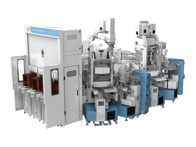
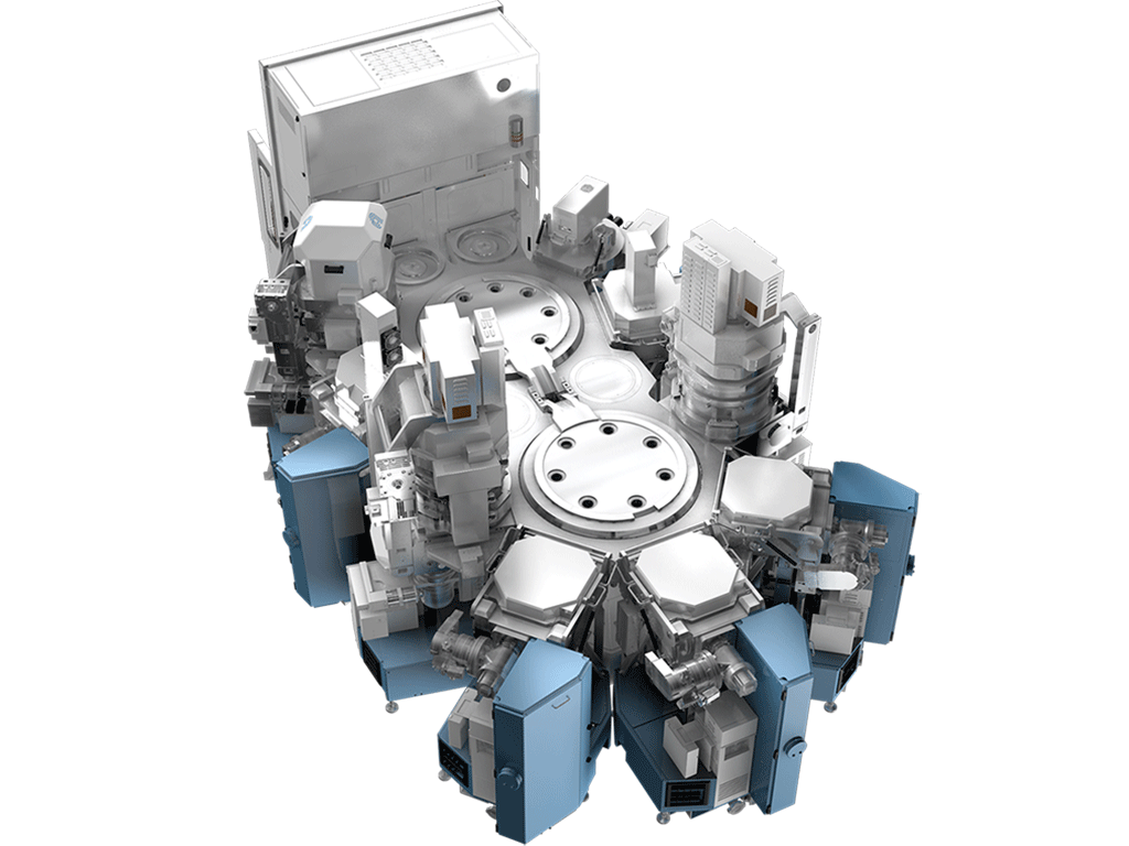
Though the tempo of Moore’s Regulation has undeniably slackened within the final decade, transistor density continues to be rising with each new course of expertise. However there’s a problem with feeding energy to smaller transistors, as with the smaller transistors comes thinner energy wires throughout the chip, which will increase their resistance and will trigger yield loss. Trying to fight that impact, this week Utilized Supplies launched its new Utilized Endura Copper Barrier Seed IMS with Volta Ruthenium Copper Vapor Deposition (CVD) instrument, which allows chipmakers to maintain utilizing copper for wiring with 2 nm-class and extra superior course of applied sciences.
Right now’s superior logic processors have about 20 layers of metallic, with skinny sign wires and thicker energy wires. Cutting down wiring with shrinking transistors presents quite a few challenges. Thinner wires have larger electrical resistance, whereas nearer wires heighten capacitance and electrical crosstalk. The mixture of the 2 can result in elevated energy consumption whereas additionally limiting efficiency scaling, which is especially problematic for datacenter grade processors that want to have all of it. Transferring energy rails to a wafer’s back-side is predicted to boost efficiency and effectivity by lowering wiring complexity and releasing up area for extra transistors.
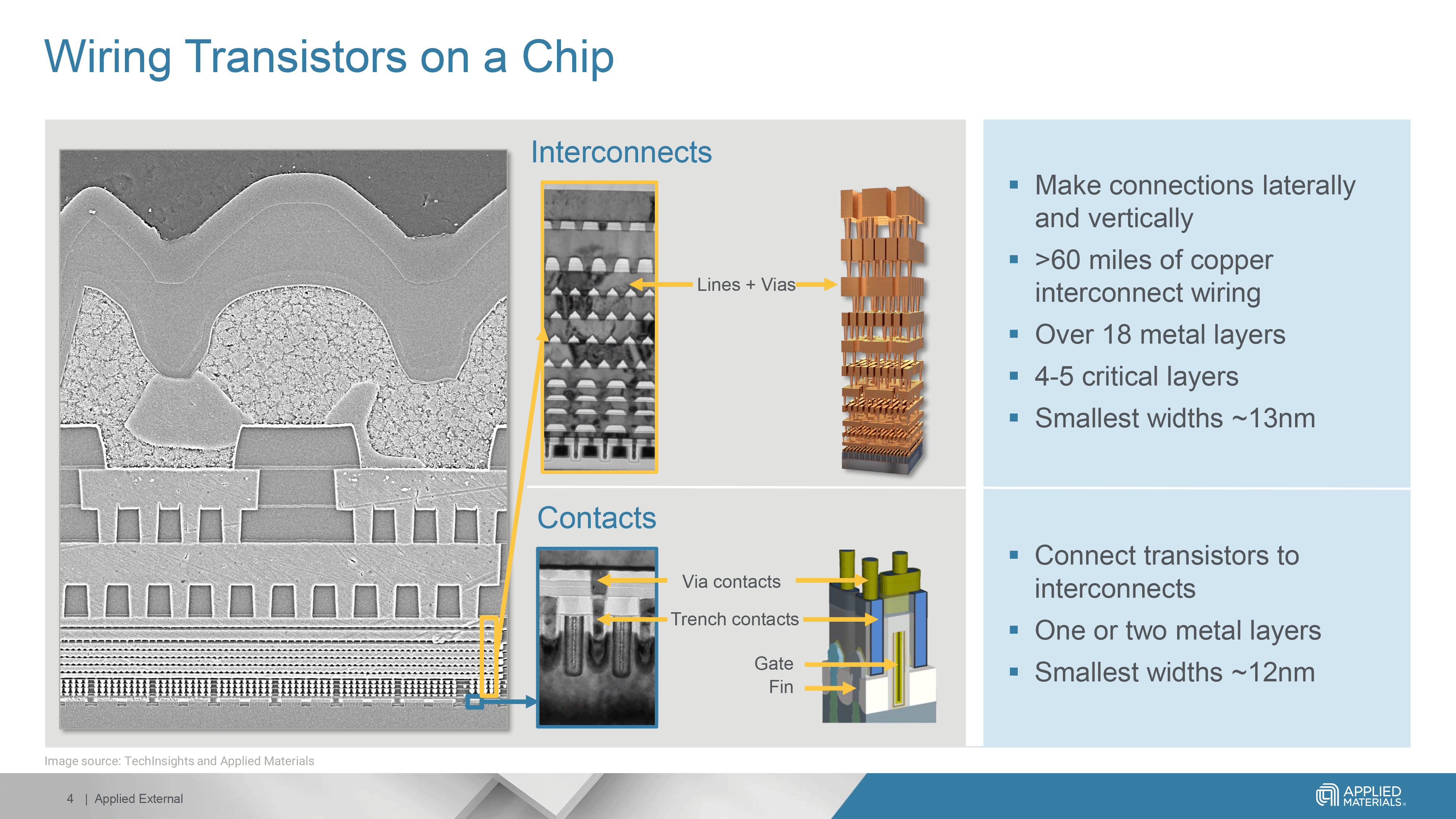
However bottom energy supply community (BSPDN) doesn’t remedy the issue with skinny wires on the whole. As lithographic scaling progresses, each transistor options and wiring trenches change into smaller. This discount implies that boundaries and liners take up more room in these trenches, leaving inadequate room to deposit copper with out creating voids, which raises resistance and may decrease yields. Moreover, the nearer proximity of wires thins the low-k dielectrics, making them extra susceptible to break throughout the etching course of. This injury will increase capacitance and weakens the chips, making them unsuitable for 3D stacking. Consequently, because the trade advances, copper wiring faces vital bodily scaling challenges. However Utilized Supplies has an answer.
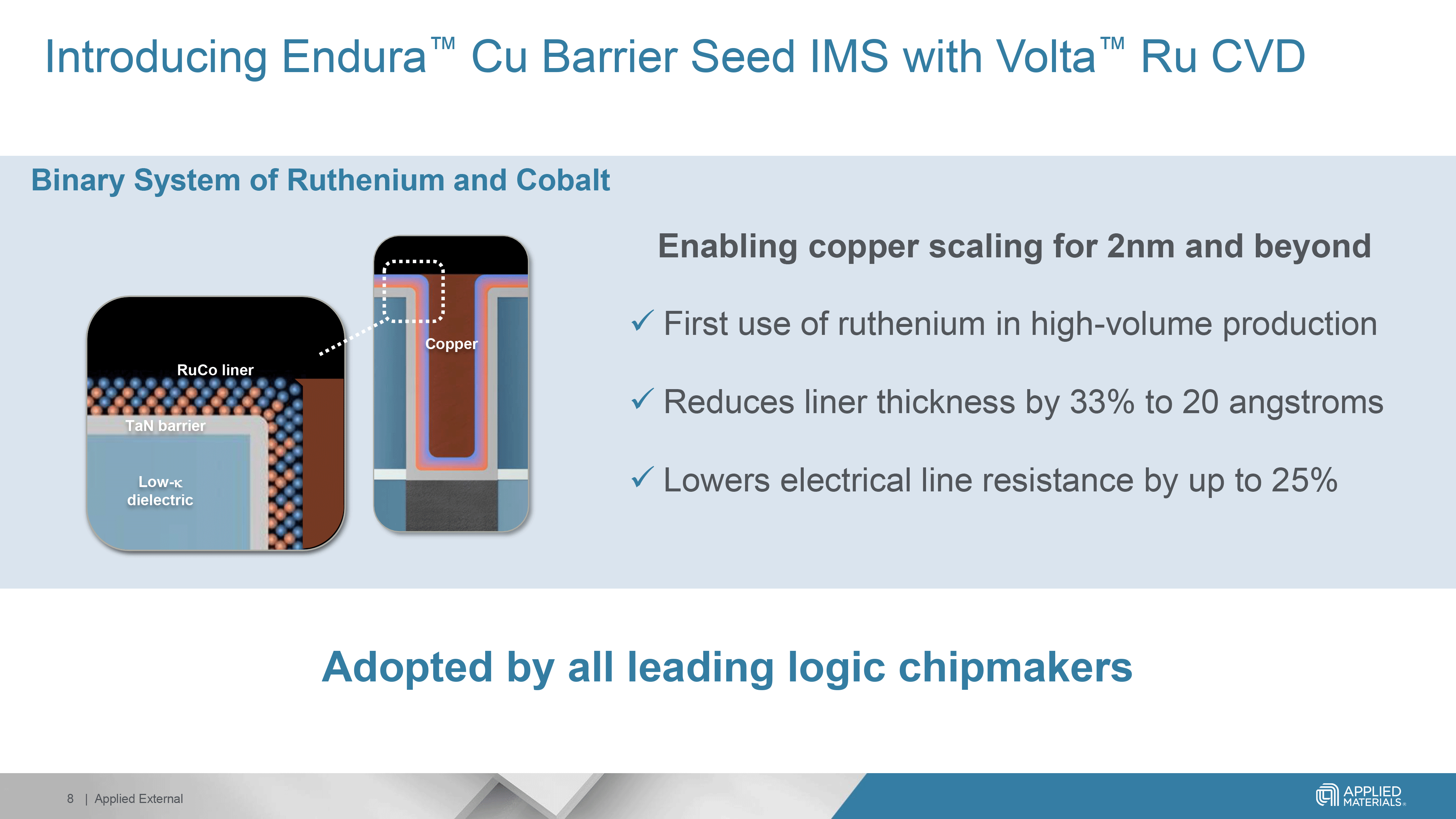
Adopting Binary RuCo Liners
Modern manufacturing applied sciences use reflow to fill interconnects with copper, the place anneals assist the copper move from the wafer floor into wiring trenches and vias. This course of is dependent upon the liners on which the copper flows. Usually, a CVD cobalt movie was used for liners, however this movie is just too thick for 3nm-class nodes (which might have an effect on resistance and yield).
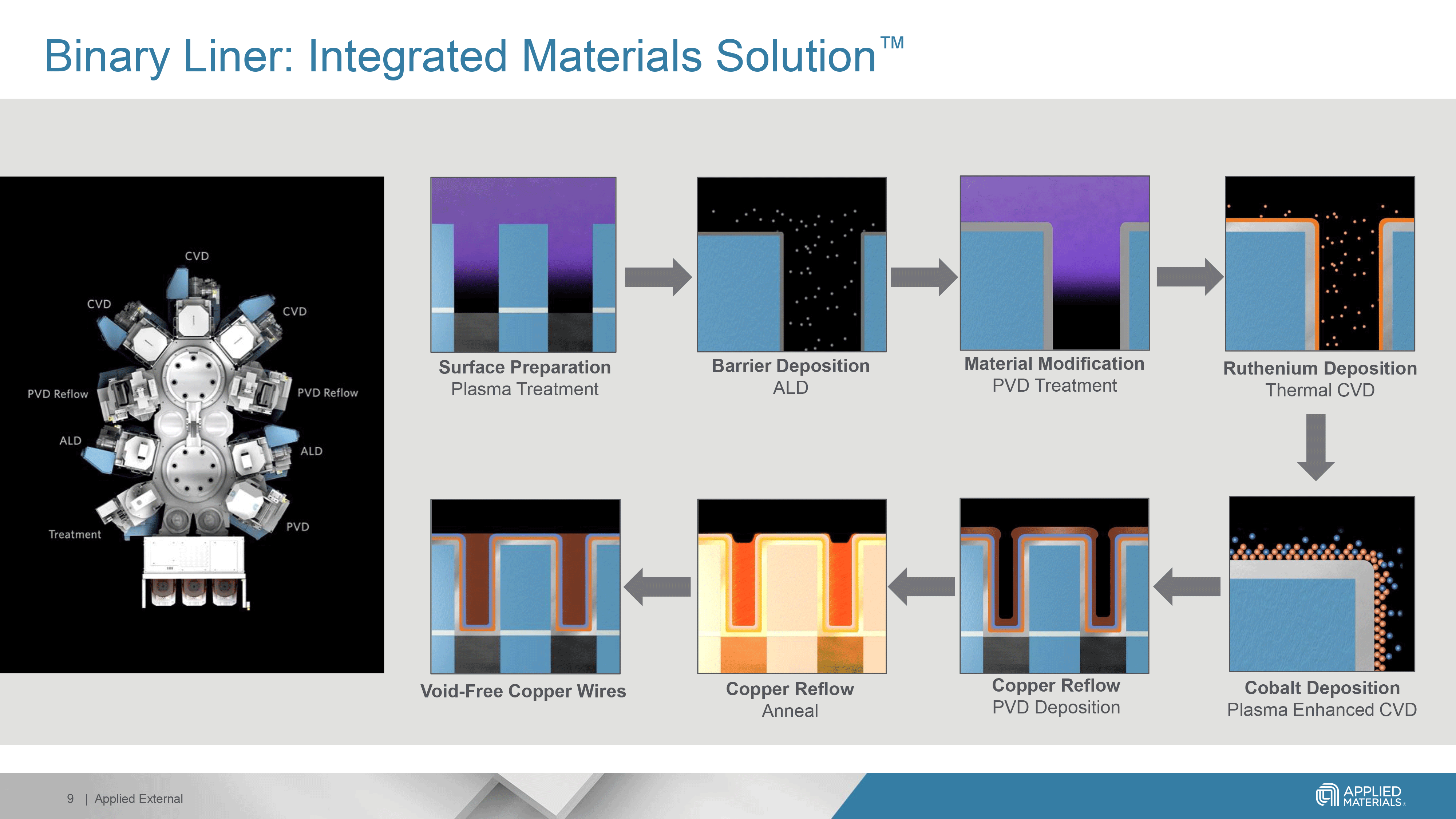
Utilized Supplies proposes utilizing a ruthenium cobalt (RuCo) binary liner with a thickness beneath 20A (2nm, 20 angstroms), which would offer higher floor properties for copper reflow. This might finally permit for 33% more room for void-free conductive copper to be reflowed, lowering the general resistance by 25%. Whereas utilization of the brand new liner requires new tooling, it could allow higher interconnects that imply larger efficiency, decrease energy consumption and better yields.
Utilized Supplies says that thus far its new Endura Copper Barrier Seed IMS with Volta Ruthenium CVD instrument has been adopted by all main logic makers, together with TSMC and Samsung Foundry for his or her 3nm-class nodes and past.
“The semiconductor trade should ship dramatic enhancements in energy-efficient efficiency to allow sustainable progress in AI computing,” stated Dr. Y.J. Mii, Government Vice President and Co-Chief Working Officer at TSMC. “New supplies that cut back interconnect resistance will play an necessary function within the semiconductor trade, alongside different improvements to enhance total system efficiency and energy.”
New Low-Okay Dielectric
However skinny and environment friendly liner shouldn’t be the one factor essential for wiring at 3nm manufacturing nodes and past. Trenches for wiring are filed not solely with a Co/RuCo liner and a Ta/N barrier, however with low dielectric fixed (Low-Okay) movie to reduce electrical cost buildup, cut back energy consumption, and decrease sign interference. Utilized Supplies has supplied its Black Diamond Low-Okay movie because the early 2000s.
However new manufacturing nodes require higher dielectrics, so this week the corporate launched an upgraded model of Black Diamond materials and a plasma-enhanced chemical vapor deposition (PEVCD) instrument to use it, the Producer Black Diamond PECVD sequence. This new materials permits for scaling all the way down to 2nm and past by additional lowering the dielectric fixed whereas additionally rising the mechanical power of the chips, which is nice for 3D stacking each for logic and reminiscence. The brand new Black Diamond is being quickly adopted by main logic and DRAM chipmakers, Utilized says.
“The AI period wants extra energy-efficient computing, and chip wiring and stacking are crucial to efficiency and energy consumption,” stated Dr. Prabu Raja, President of the Semiconductor Merchandise Group at Utilized Supplies. “Utilized’s latest built-in supplies answer allows the trade to scale low-resistance copper wiring to the rising angstrom nodes, whereas our newest low-k dielectric materials concurrently reduces capacitance and strengthens chips to take 3D stacking to new heights.”