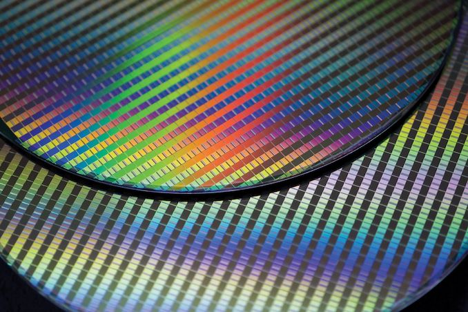
TSMC's Roadmap at a Look: N3X, N2P, A16 Coming in 2025/2026

As introduced final week by TSMC, later this 12 months the corporate is about to start out high-volume manufacturing on its N3P fabrication course of, and this would be the firm's most superior node for some time. Subsequent 12 months issues will get a bit extra attention-grabbing as TSMC can have two course of applied sciences that would truly compete in opposition to one another after they enter high-volume manufacturing (HVM) within the second half of 2025.
| Marketed PPA Enhancements of New Course of Applied sciences Knowledge introduced throughout convention calls, occasions, press briefings and press releases |
|||||||||
| Compiled by AnandTech |
TSMC | ||||||||
| N3 vs N5 |
N3E vs N5 |
N3P vs N3E |
N3X vs N3P |
N2 vs N3E |
N2P vs N3E |
N2P vs N2 |
A16 vs N2P |
||
| Energy | -25% -30% |
-34% | -5% -10% |
-7%*** | -25% -30% |
-30% -40% |
-5% -10% |
-15% -20% |
|
| Efficiency | +10% +15% |
+18% | +5% | +5% Fmax @1.2V** |
+10% +15% |
+15% +20% |
+5 +10% |
+8% +10% |
|
| Density* | ? | 1.3x | 1.04x | 1.10x*** | 1.15x | 1.15x | ? | 1.07x 1.10x |
|
| HVM | This fall 2022 |
This fall 2023 |
H2 2024 |
H2 2025 |
H2 2025 |
H2 2026 |
H2 2026 |
H2 2026 |
|
*Chip density revealed by TSMC displays 'blended' chip density consisting of fifty% logic, 30% SRAM, and 20% analog.
**On the identical space.
***On the identical velocity.
The manufacturing nodes are N3X (3nm-class, excessive performance-focused) in addition to N2 (2nm-class). TSMC says that when in comparison with N3P, chips made on N3X can both decrease energy consumption by 7% on the identical frequency by reducing Vdd from 1.0V to 0.9V, enhance efficiency by 5% on the identical space, or enhance transistor density by round 10% on the identical frequency. In the meantime, the important thing benefit of N3X in comparison with predecessors is its most voltage of 1.2V, which is essential for ultra-high-performance functions, corresponding to desktop or datacenter GPUs.
TSMC's N2 will probably be TSMC's first manufacturing node to make use of gate-all-around (GAA) nanosheet transistors and it will considerably improve its efficiency, energy, and space (PPA) traits. When in comparison with N3E, semiconductors produced on N3 can reduce their energy consumption by 25% – 30% (on the identical transistor rely and frequency), enhance their efficiency by 10% – 15% (on the identical transistor rely and energy), and enhance transistor density by 15% (on the identical velocity and energy).
Whereas N2 will definitely be TSMC's undisputed champ on the subject of energy consumption and transistor density, N3X may probably problem it on the subject of efficiency, particularly at excessive voltages. For a lot of clients N3X can even have a advantage of utilizing confirmed FinFET transistors, so N2 won’t be robotically the most effective of TSMC's nodes within the second half of 2025.
2026: N2P and A16
Within the following 12 months TSMC will once more supply two nodes which might be set to focus on usually comparable smartphone and high-performance computing functions: N2P (performance-enhanced 2nm-class) and A16 (1.6nm-class with bottom energy supply).
N2P is predicted to ship a 5% – 10% decrease energy (on the identical velocity and transistor rely) or a 5% – 10% greater efficiency (on the identical energy and transistor rely) in comparison with the unique N2. In the meantime, A16 is about to supply an as much as 20% decrease energy (on the identical velocity and transistors), as much as 10% greater efficiency (on the identical energy and transistors), and as much as 10% greater transistor density in comparison with N2P.
Protecting in thoughts that A16 options enhanced bottom energy supply community, it would possible be the node of alternative for performance-minded chip designers. However in fact, will probably be costlier to make use of A16 due to the bottom energy supply, which requires extra course of steps.