ASML Patterns First Wafer Utilizing Excessive-NA EUV Device, Ships Second Excessive-NA Scanner
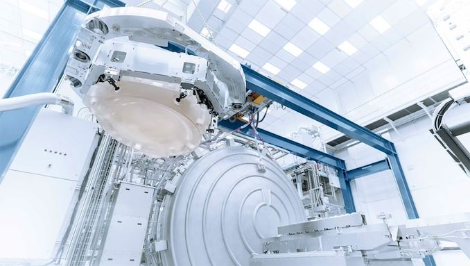
This week ASML is making two crucial bulletins associated to their progress with excessive numerical aperature excessive ultraviolet lithography (Excessive-NA EUV). First up, the corporate’s Excessive-NA EUV prototype system at its fab in Veldhoven, the Netherlands, has printed the primary 10nm patterns, which is a significant milestone for ASML and their next-gen instruments. Second, the corporate has additionally revealed that it is second Excessive-NA EUV system is now out the door as properly, and has been shipped to an unnamed buyer.
“Our Excessive-NA EUV system in Veldhoven printed the first-ever 10 nanometer dense strains,” an announcement by ASML reads. “Imaging was achieved after optics, sensors and levels accomplished coarse calibration. Subsequent up: bringing the system to full efficiency. And attaining the identical ends in the sphere.”
Our Excessive NA EUV system in Veldhoven printed the first-ever 10 nanometer dense strains.
Imaging was achieved after optics, sensors and levels accomplished coarse calibration.
Subsequent up: bringing the system to full efficiency. And attaining the identical ends in the sphere.
pic.twitter.com/zcA5V0ScUf
— ASML (@ASMLcompany) April 17, 2024
Alongside the system shipped to Intel at the end of 2023, ASML has retained their very own Twinscan EXE:5000 scanner at their Veldhoven, Netherlands, facility, which is what the corporate is utilizing for additional analysis and improvement into Excessive-NA EUV. Utilizing that machine, the corporate has been in a position to print dense strains spaced 10 nanometers aside, which is a significant milestone in photolithography improvement. Beforehand, solely small-scale, experimental lab machines have been in a position to obtain this type of a decision. Ultimately, Excessive-NA EUV instruments will obtain a decision of 8 nm, which shall be instrumental to construct logic chips on applied sciences past 3 nm.
Intel’s Twinscan EXE:5000 scanner at its D1X fab close to Hillsboro, Oregon can also be shut behind, and its meeting is claimed to be nearing completion. That machine shall be primarily used for Intel’s personal Excessive-NA EUV R&D, with Intel slated to make use of its successor — the commercial-grade Twinscan EXE:5200 — to supply its chips on its Intel 14A (1.4 nm-class) in mass portions in 2026 – 2027.
However Intel won’t be the one chipmaker that will get to experiment with a Excessive-NA EUV scanner for very lengthy. As revealed by ASML, the corporate not too long ago began transport one other Twinscan EXE:5000 machine to yet one more buyer. The fab instrument maker just isn’t disclosing the consumer, however beforehand it has stated that every one of main logic and reminiscence producers are within the means of procuring Excessive-NA instruments for R&D functions, so the checklist of ‘suspects’ is fairly quick.
“Concerning Excessive-NA, or 0.55 NA EUV, we shipped our first system to a buyer and this technique is at the moment beneath set up,” said Christophe Fouquet, chief enterprise officer of ASML, on the firm’s earnings convention name with analysts and buyers. “We began to ship the second system this month and its set up can also be about to start out.”
Whereas Intel plans to undertake Excessive-NA EUV instruments forward of the trade, different chipmakers appear to a bit extra cautious and plan to depend on dangerous but already recognized Low-NA EUV double patterning methodology for manufacturing a 3 nm and a couple of nm. Nonetheless, whatever the precise timing for a transition, the entire main fabs shall be counting on Excessive-NA EUV instruments in due time. So all events have an curiosity in how ASML’s R&D seems.
“The shopper curiosity for our [High-NA] system lab is excessive as this technique will assist each our Logic and Reminiscence prospects put together for Excessive-NA insertion into their roadmaps,” stated Fouquet. “Relative to 0.33 NA, the 0.55 NA system supplies finer decision enabling an virtually 3x enhance in transistor density, at the same productiveness, in help of sub-2nm Logic and sub-10nm DRAM nodes.”


