Going Larger and Aiming Greater In AI Market
Intel this morning is kicking off the second day of their Vision 2024 conference, the corporate’s annual closed-door enterprise and customer-focused get-together. Whereas Imaginative and prescient is just not sometimes a hotbed for brand new silicon bulletins from Intel – that’s extra of an Innovation factor within the fall – attendees of this yr’s present are usually not coming away empty handed. With a heavy deal with AI occurring throughout the {industry}, Intel is utilizing this yr’s occasion to formally introduce the Gaudi 3 accelerator, the next-generation of Gaudi high-performance AI accelerators from Intel’s Habana Labs subsidiary.
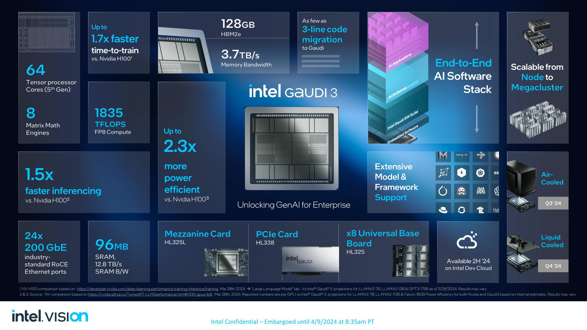
The newest iteration of Gaudi can be launching within the third quarter of 2024, and Intel is already transport samples to prospects now. The {hardware} itself is one thing of a combined bag in some respects (extra on that in a second), however with 1835 TFLOPS of FP8 compute throughput, Intel believes it’s going to be greater than sufficient to carve off a bit of the expansive (and costly) AI marketplace for themselves. Primarily based on their inside benchmarks, the corporate expects to find a way beat NVIDIA’s flagship Hx00 Hopper structure accelerators in at the very least some important giant language fashions, which can open the door to Intel grabbing a bigger piece of the AI accelerator market at a important time within the {industry}, and a second when there merely isn’t sufficient NVIDIA {hardware} to go round.
The upcoming launch of Gaudi 3 additionally comes amidst a change in how Intel is positioning its AI accelerator merchandise – one which has seen the Gaudi lineup elevated to Intel’s flagship server accelerator. Historically downplayed in favor of Intel’s GPU Knowledge Heart Max merchandise (Ponte Vecchio), Habana Labs and Gaudi have gained a brand new respect inside Intel following the cancellation of Rialto Bridge in favor of the 2025 release of Falcon Shores. In brief, Intel doesn’t have every other new AI accelerator silicon popping out apart from Gaudi 3, so Intel goes to struggle with the chip that it has.
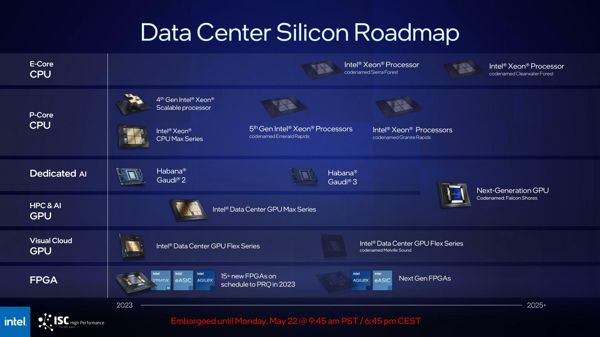
Intel 2023 Knowledge Heart Silicon Roadmap
Which isn’t to knock Habana Labs or Gaudi 3 upfront. Intel thinks they’ll win right here on efficiency; if they’ll, that’s a giant deal. However it is a product that’s clearly been uplifted from a side-project below the Intel umbrella to a front-and-center processor. So the scope of Gaudi 3’s skills, {hardware}, and how much markets Intel is chasing, is narrower than we’ve seen with a few of their different flagship merchandise.
| Gaudi Accelerator Specification Comparability | |||||
| Gaudi 3 | Gaudi 2 | Gaudi (1) | |||
| Matrix Math Engines | 8 | 2 | 1 | ||
| Tensor Cores | 64 | 24 | 8 | ||
| Clockspeed | ? | ? | ? | ||
| Reminiscence Clock | 3.7Gbps HBM2e | 3.27Gbps HBM2e | 2Gbps HBM2 | ||
| Reminiscence Bus Width | 2x 4096-bit | 6144-bit | 4096-bit | ||
| Reminiscence Bandwidth | 3.7TB/sec | 2.45TB/sec | 1TB/sec | ||
| VRAM | 128GB (2x 64GB) |
96GB | 32GB | ||
| FP8 | 1835 TFLOPS | 920 TFOPS? | N/A | ||
| BF16 | 920 TFLOPS? | 230 TFLOPS? | ? TFLOPS | ||
| Interconnect | 200Gb Ethernet 24 Hyperlinks (600GB/sec) |
100Gb Ethernet 24 Hyperlinks (300GB/sec) |
100Gb Ethernet 10 Hyperlinks (120GB/sec) |
||
| Processor | Gaudi 3 | Gaudi 2 | Gaudi (1) | ||
| Transistor Depend | 2x (So much) | ? | ? | ||
| TDP | 900W | 600W | 350W | ||
| Manufacturing Course of | TSMC 5nm | TSMC 7nm | TSMC 16nm | ||
| Interface | OAM 2.0 | OAM 1.1 | OAM | ||
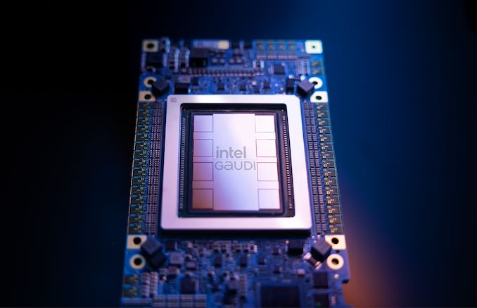
Diving in to the {hardware} itself, let’s check out Gaudi 3.
Gaudi 3 is a direct evolution of the Gaudi 2 {hardware}. Habana Labs has settled on an structure they like and contemplate profitable, so Gaudi 3 isn’t orchestrating a large overhaul of their structure (that can include Falcon Shores). The flip aspect to that, nevertheless, is that there’s not a ton to speak about right here when it comes to new options – or options that Intel needs to reveal, at the very least – so at a excessive degree, Gaudi 3 is extra of a superb factor.
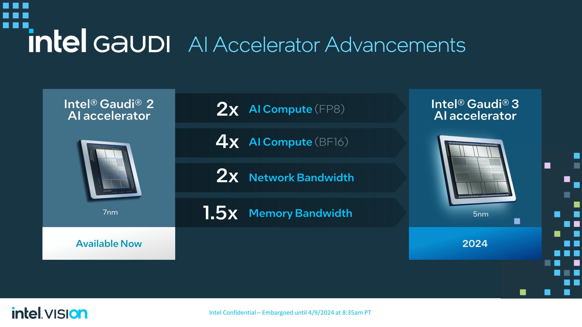
With the previous-generation Gaudi 2 accelerator being constructed on TSMC’s 7nm course of, Habana has introduced Gaudi 3 to the newer 5nm course of. The Gaudi 3 die, in flip, has added a modest quantity of computational {hardware}, increasing from 2 Matrix Math Engines and 24 Tensor Cores to 4 Matrix Math Engines and 32 Tensor cores. Given the restricted structure modifications with Gaudi 3, I’m presuming that these tensor cores are nonetheless 256 byte-wide VLIW SIMD models, as they had been in Gaudi 2.
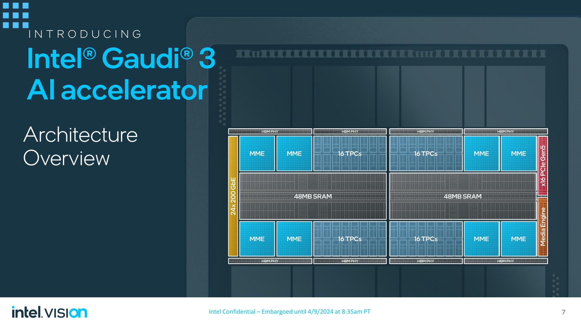
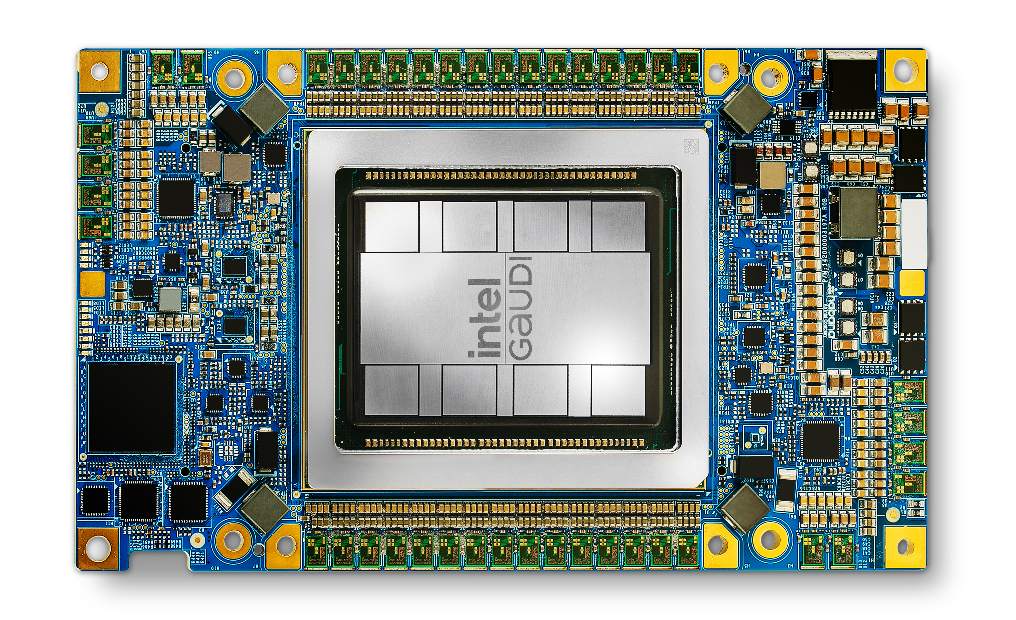
Whereas Intel isn’t disclosing the whole transistor depend of the Gaudi 3 die, the restricted addition of recent {hardware} has made Gaudi 3 sufficiently small that Intel has been capable of pack two dies on to a single chip, making the complete Gaudi 3 accelerator a dual-die setup. Much like NVIDIA’s just lately introduced Blackwell accelerator, two equivalent dies are positioned on a single package deal, and are linked through a excessive bandwidth hyperlink in an effort to give the chip a unified reminiscence tackle house. Based on Intel, the mixed dies will behave as a single chip, although as the corporate isn’t disclosing any important particulars on the die-to-die hyperlink connecting the chips, it stays unclear simply how a lot bandwidth is definitely accessible to cross the dies, and at what latency.
In a rarity for the Habana crew, they’ve disclosed the whole throughput of the chip for FP8 precision: 1835 TFLOPS, which is twice the FP8 efficiency of Gaudi 2. Extra fascinating is that BF16 efficiency has apparently elevated by 4x over Gaudi 2, nevertheless Intel hasn’t disclosed an official throughput quantity for that mode, or what architectural modifications have led to that enchancment. Both means, Intel wants to maximise the efficiency of Gaudi 3 in the event that they’re going to carve off a bit of the AI marketplace for themselves.
Feeding the beast is an oddly outdated HBM2e reminiscence controller, the identical reminiscence kind supported by Gaudi 2. Whereas Intel might be a smidge too early for HBM3E, I’m very stunned to not see HBM3 supported, each for the higher reminiscence bandwidth and higher reminiscence capability the HBM3 lineage affords. Because of sticking with HBM2e, the best capability stacks accessible are 16GB, giving the accelerator a complete of 128GB of reminiscence. That is clocked at 3.7Gbps/pin, for a complete reminiscence bandwidth of three.7TB/second. Every Gaudi 3 die provides 4 HBM2e PHYs, bringing the chip’s complete to eight stacks of reminiscence.
In the meantime, every Gaudi 3 die has 48MB of SRAM on-board, giving the entire chip 96MB of SRAM. Based on Intel, the combination SRAM bandwidth is 12.8TB/second.
Intel is just not disclosing the clockspeed of the Gaudi 3 accelerator (nor did they ever disclose Gaudi 2’s, for that matter). Nonetheless on condition that Intel has greater than doubled the {hardware} on-hand, we’re probably taking a look at decrease clockspeeds total. Even with the smaller 5nm die, two dies means a complete lot extra transistors to feed, and never a ton of extra energy to do it.
On that observe, the TDP for the fundamental, air-cooled Gaudi 3 accelerator is 900 Watts, 50% greater than the 600W restrict of its predecessor. Intel is making use of the OAM 2.0 kind issue right here, which affords the next energy restrict than OAM 1.x (700W). Nonetheless, Intel can be creating and qualifying liquid-cooled variations of Gaudi 3, which can supply greater efficiency in alternate for even greater TDPs. All types of Gaudi 3 will use PCIe backhaul to hook up with their host CPU, with Gaudi 3 sporting a PCIe Gen 5 x16 hyperlink.
Broadly talking, the restricted particulars on the Gaudi structure remind me quite a lot of AMD’s Instinct MI250X accelerator. That CDNA 2 half was in some ways a pair of die-shrunk MI100s positioned collectively on a single chip, bringing few new architectural options, however a complete lot extra silicon to do the heavy lifting. Critically, nevertheless, MI250X introduced itself as two accelerators (regardless of the Infinity Cloth hyperlinks between the dies), whereas Gaudi 3 is meant to behave as a single unified accelerator.
Networking: Ethernet Taken To The Excessive
Outdoors of the core structure of the Gaudi 3, Habana’s different large technological improve with Gaudi 3 has been on the I/O aspect of issues. Going again to the earliest days of Gaudi, Habana has relied on an all-Ethernet structure for his or her chips, utilizing Ethernet for each on-node chip-to-chip connectivity, and scale-out node-to-node connectivity. It’s basically the inverse of what NVIDIA has performed, scaling Ethernet all the way down to the chip degree, quite than scaling NVLink as much as the rack degree.
Gaudi 2 supplied 24 100Gb Ethernet hyperlinks per chip; Gaudi 3 doubles the bandwidth of these hyperlinks to 200Gb/second, giving the chip a complete exterior Ethernet I/O bandwidth of 8.4TB/second cumulative up/down.
The really helpful topology for Gaudi 3 – and what Intel can be using in their very own baseboards – is a 21/3 cut up. 21 hyperlinks can be used for on-node, chip-to-chip connectivity, with 3 hyperlinks going to every of the opposite 7 Gaudi 3 accelerators on a totally populated 8-way node.
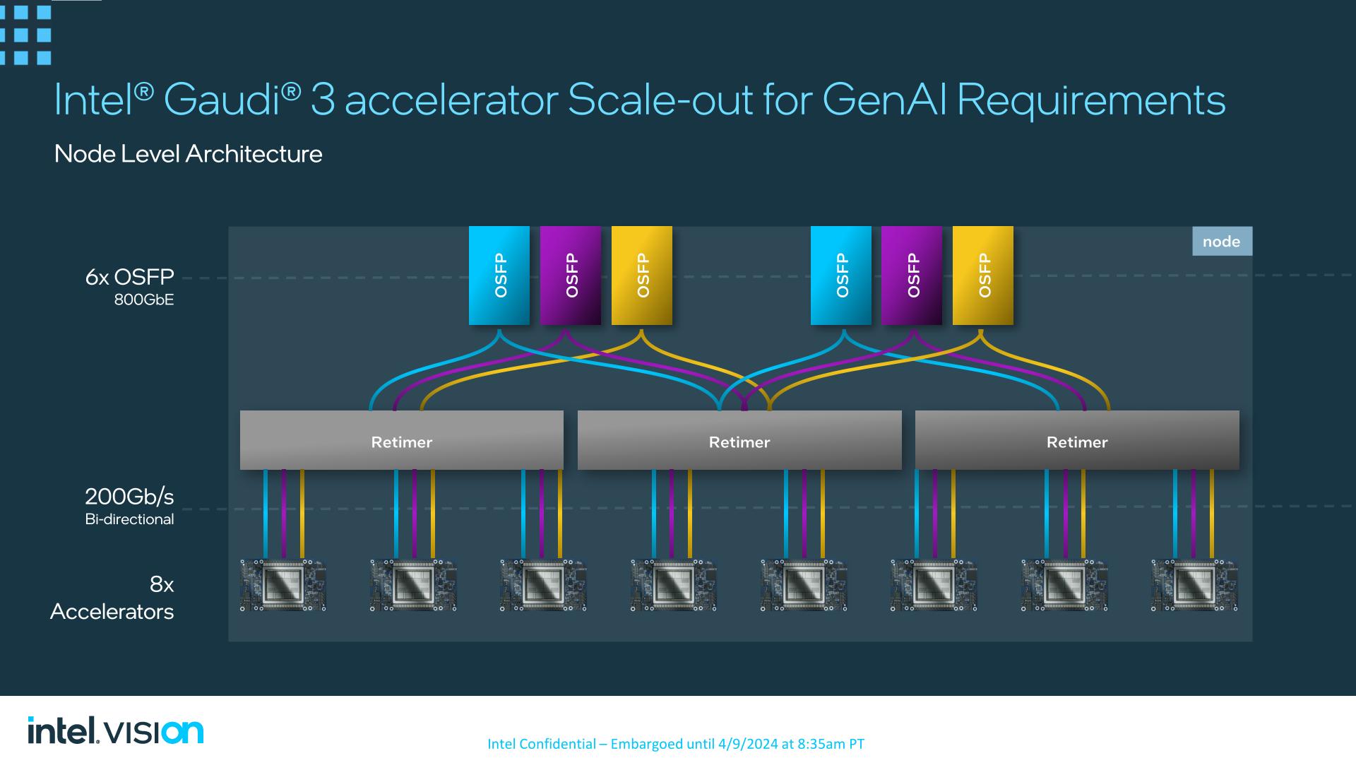
The remaining 3 hyperlinks from every chip, in the meantime, can be used to feed a sextet of 800Gb Octal Small Type Issue Pluggable (OSFP) Ethernet hyperlinks. By way of using retimers, the ports can be cut up up in blocks of two, after which balanced over 5 accelerators.
Finally, Intel is seeking to push the scalability of Gaudi 3 right here, each when it comes to efficiency and marketability. With the biggest of LLMs requiring many nodes to be linked collectively to kind a single cluster to offer the mandatory reminiscence and compute efficiency for coaching, the most important prospects that Intel is chasing with Gaudi 3 will want an AI accelerator that may scale out to those giant sizes – and thus giving Intel loads of alternative to promote an equally giant variety of accelerators. All of the whereas, by embracing a pure Ethernet setup, Intel is banking on successful over prospects who don’t need to spend money on proprietary/different interconnects comparable to InfiniBand.
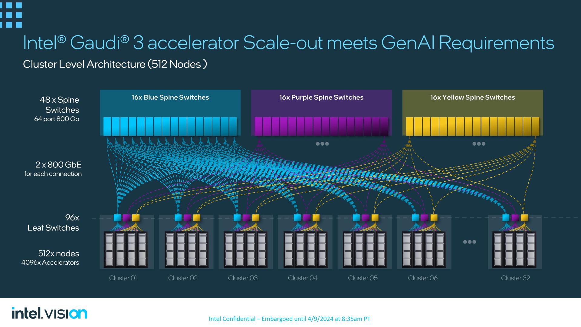
Finally, Intel has networking topologies for as many as 512 nodes already developed, utilizing 48 backbone switches to attach as much as 32 clusters – every of which homes 16 nodes. And based on Intel, Gaudi 3 can nonetheless scale additional than that, out to 1000’s of nodes.
Efficiency: Beating H100 At Llamas and Falcons
All through the lifetime of the Gaudi accelerators, Intel and Habana have most well-liked to deal with speaking concerning the efficiency of the chips as a substitute of simply the specs, and for Gaudi 3 that isn’t altering. With the majority of Imaginative and prescient’s attendees being enterprise clientele, Intel is seeking to make a splash with benchmark-based efficiency figures that reveal what Gaudi 3 can truly do.
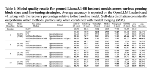
I’m not going to spend an excessive amount of time going over these since they’re primarily aggressive efficiency claims that we will’t validate. But it surely’s noteworthy right here that the Gaudi crew opted to go straight at NVIDIA right here by utilizing their very own benchmarks and end result units. In different phrases, the Gaudi efficiency figures supplied by Intel are plotted towards NVIDIA’s personal self-reported figures, quite than Intel cooking up situations to drawback NVIDIA. That stated, it should even be famous that these are efficiency projections, and never measured efficiency of assembled programs (and I doubt Intel has 8192 Gaudi 3s sitting round for this).
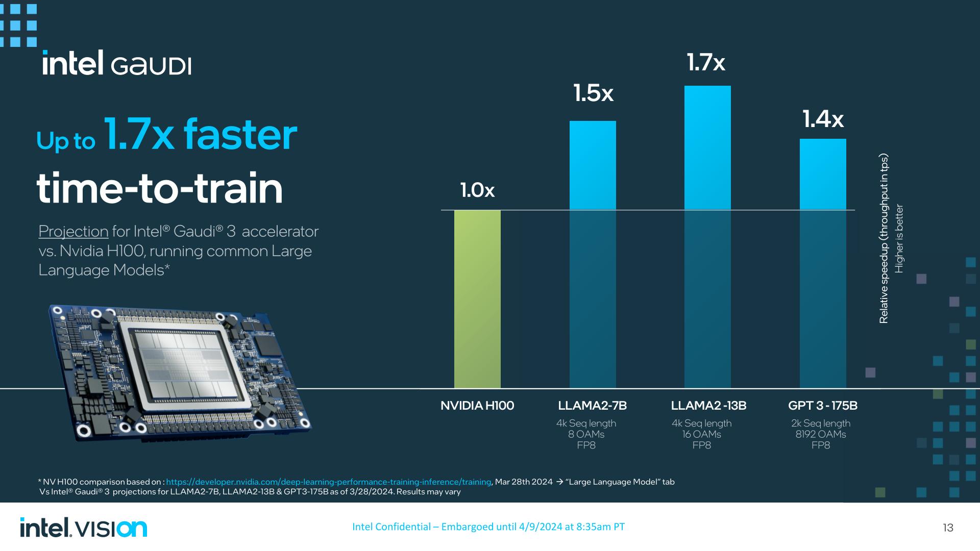
In comparison with H100, Intel is claiming that Gaudi 3 ought to beat H100 by as much as 1.7x in coaching Llama2-13B in a 16 accelerator cluster at FP8 precision. Despite the fact that H100 is developing on 2 years outdated, beating H100 at coaching something by a big diploma can be a giant win for Intel if it pans out.
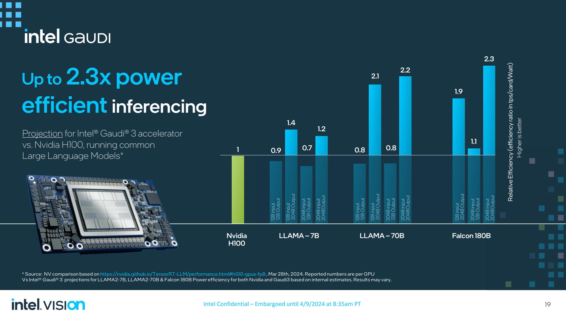
In the meantime, Intel is projecting 1.3x to 1.5x the inferencing efficiency of H200/H100 with Gaudi 3, and maybe most notably, at as much as 2.3x the ability effectivity.
As at all times, nevertheless, the satan is within the particulars. Intel nonetheless loses to the H100 at instances in these inference workloads – notably these with out 2K outputs – so the Gaudi 3 is way from a clear sweep. And, after all, there are the entire benchmark outcomes that Intel isn’t selling.
To Intel’s credit score, nevertheless, they’re the one different main {hardware} producer who has been offering MLPerf outcomes as of late. So nevertheless Gaudi 3 will carry out (and the way Gaudi 2 presently performs), they’ve been way more above-board than most in publishing outcomes for industry-standard checks.
OAM and PCIe Playing cards Launching In Second-Half of 2024
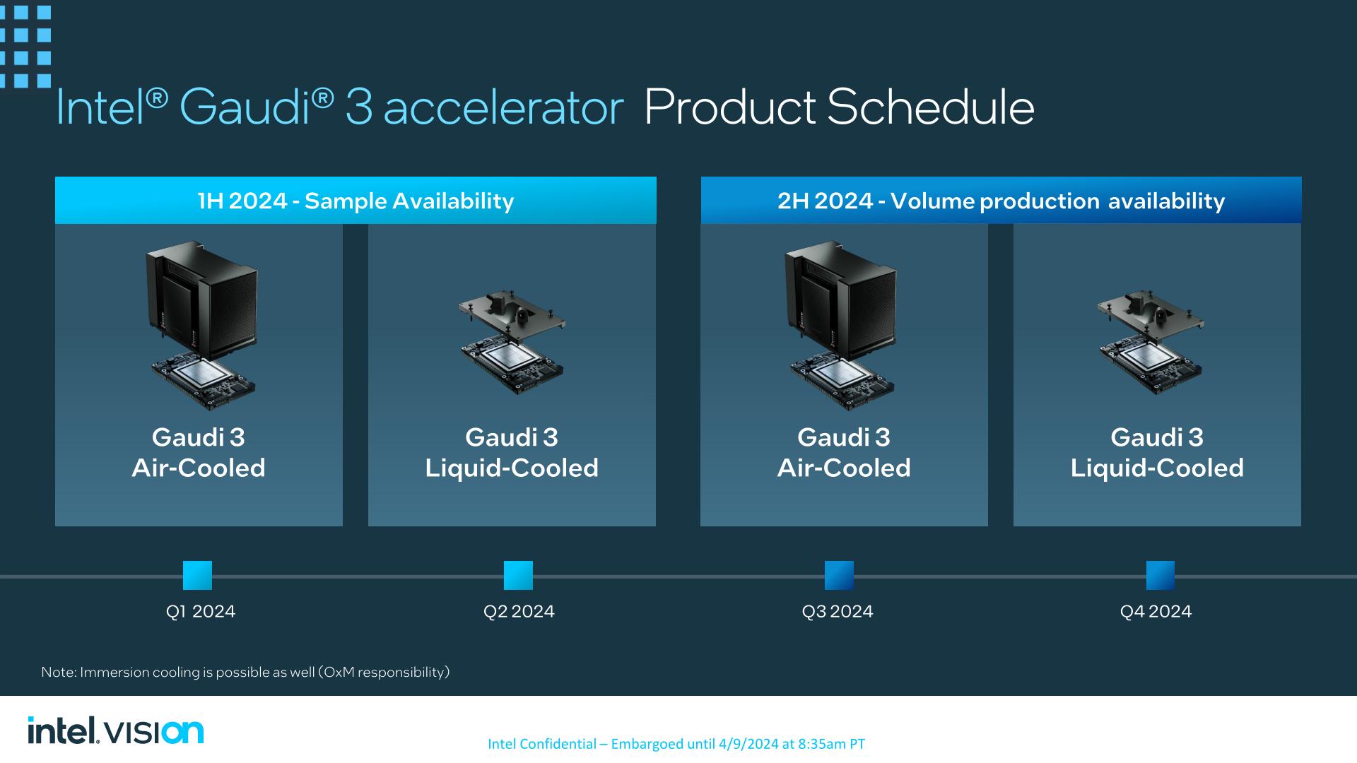
Wrapping issues up, Intel can be releasing their first Gaudi 3 merchandise within the subsequent quarter. The corporate already has air-cooled variations of the OEAM accelerator of their labs for qualification and out to prospects for sampling, in the meantime the liquid-cooled variations can be sampling this quarter.
Lastly, in a primary time for the Gaudi crew, Intel can be providing a model of Gaudi 3 in a extra conventional PCIe kind issue as effectively. The HL-338 card is a ten.5-inch full peak dual-slot PCIe card. It provides the entire identical {hardware} because the OAM Gaudi 3, proper on all the way down to the height efficiency of 1835 TFLOPS FP8. Nonetheless it is going to ship with a much more PCIe-slot pleasant TDP of 600 Watts – 300 Watts lower than the OAM card – so sustained efficiency ought to be notably decrease.
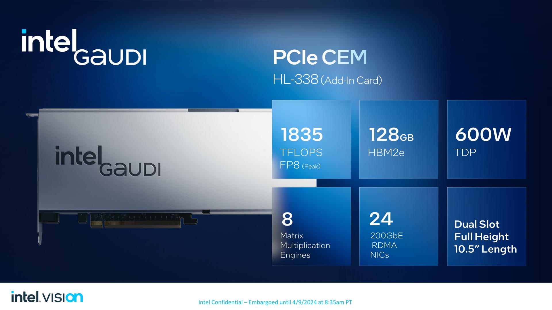
Although not pictured in Intel’s slide, the PCIe playing cards supply two 400Gb Ethernet ports for scale-out configurations. In the meantime Intel can be providing a “high board” for the PCIe playing cards that, much like NVIDIA’s NVLink bridges, can hyperlink as much as 4 of them for inter-card communication. The OAM kind issue will stay the best way to go for each highest efficiency on a per-accelerator foundation and to maximise scale-out potential, however for purchasers who want one thing to plug and go in conventional PCIe slots, there may be lastly an possibility for that for a Gaudi accelerator.
The PCIe model of the Gaudi 3 is about to launch within the 4th quarter of this yr, alongside the liquid cooled model of the OAM module.