SK Hynix Mulls Constructing $4 Billion Superior Packaging Facility in Indiana
SK hynix is contemplating whether or not to construct a complicated packaging facility in Indiana, reviews the Wall Street Journal. If the corporate proceeds with the plan, it intends to speculate $4 billion in it and assemble one of many world’s largest superior packaging amenities. However to perform the venture, SK hynix expects it should need assistance from the U.S. authorities.
Acknowledging the report however stopping wanting confirming the corporate’s plans, an organization spokeswoman instructed the WSJ that SK hynix “is reviewing its superior chip packaging funding within the U.S., however hasn’t made a last resolution but.”
Firms like TSMC and Intel spend billions on superior packaging amenities, however up to now, no firm has introduced a chip packaging plant price fairly as a lot as SH hynix’s $4 billion. The sphere of superior packaging – CoWoS, passive silicon interposers, redistribution layers, die-to-die bonding, and different innovative applied sciences – has seen an explosion in demand within the final half-decade. As bandwidth advances with conventional natural packaging are largely performed out, chip designers have wanted to show to extra complicated (and troublesome to assemble) applied sciences as a way to wire up an ever bigger variety of indicators at ever-higher switch charges. Which has turned superior packaging right into a bottleneck for high-end chip and accelerator manufacturing, driving a necessity for extra packaging amenities.
If SK hynix approves the venture, the superior packaging facility is predicted to start operations in 2028 and will create as many as 1,000 jobs. With an estimated price of $4 billion, the plant is poised to grow to be one of many largest superior packaging amenities on the planet.
In the meantime, authorities backing is considered important for investments of this scale, with potential state and federal tax incentives, in line with the report. These incentives type a part of a broader initiative to bolster the U.S. semiconductor trade and reduce dependence on reminiscence produced in South Korea.
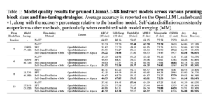
SK hynix is the world’s main producer of HBM reminiscence, and is likely one of the key HBM suppliers to NVIDIA. Subsequent generations of HBM reminiscence (together with HBM4 and HBM4E) would require even nearer collaboration between chip designers, chipmakers, and reminiscence makers. Due to this fact, packaging HBM in America may very well be a big profit for NVIDIA, AMD, and different U.S. chipmakers.
Investing within the Indiana facility will probably be a strategic transfer by SK hynix to boost its superior chip packaging capabilities on the whole and demonstrating dedication to the U.S. semiconductor trade.