Samsung Launches 12-Hello 36GB HBM3E Reminiscence Stacks with 10 GT/s Velocity
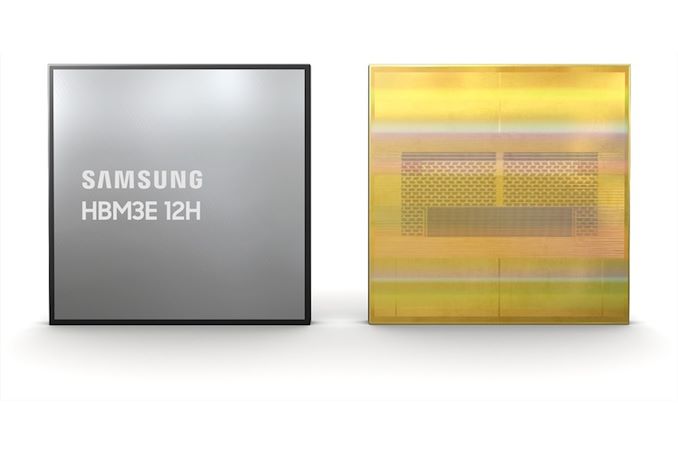
Samsung introduced late on Monday the completion of the event of its 12-Hello 36 GB HBM3E reminiscence stacks, simply hours after Micron stated it had kicked off mass production of its 8-Hi 24 GB HBM3E memory products. The brand new reminiscence packages, codenamed Shinebolt, enhance peak bandwidth and capability in comparison with their predecessors, codenamed Icebolt, by over 50% and are at the moment the world’s quickest reminiscence units.
As the outline suggests, Samsung’s Shinebolt 12-Hello 36 GB HBM3E stacks pack 12 24Gb reminiscence units on high of a logic die that includes a 1024-bit interface. The brand new 36 GB HBM3E reminiscence modules characteristic a knowledge switch fee of 10 GT/s and thus supply a peak bandwidth of 1.28 TB/s per stack, the trade’s highest per-device (or reasonably per-module) reminiscence bandwidth.
In the meantime, take into account that builders of HBM-supporting processors are typically cautious, so they are going to use Samsung’s HBM3E at a lot decrease information switch charges to a point due to energy consumption and to a point to make sure final stability for synthetic intelligence (AI) and high-performance computing (HPC) functions.
| Samsung HBM Reminiscence Generations | ||||||
| HBM3E (Shinebolt) |
HBM3 (Icebolt) |
HBM2E (Flashbolt) |
HBM2 (Aquabolt) |
|||
| Max Capability | 36GB | 24 GB | 16 GB | 8 GB | ||
| Max Bandwidth Per Pin | 9.8 Gb/s | 6.4 Gb/s | 3.6 Gb/s | 2.0 Gb/s | ||
| Variety of DRAM ICs per Stack | 12 | 12 | 8 | 8 | ||
| Efficient Bus Width | 1024-bit | |||||
| Voltage | ? | 1.1 V | 1.2 V | 1.2 V | ||
| Bandwidth per Stack | 1.225 TB/s | 819.2 GB/s | 460.8 GB/s | 256 GB/s | ||
To make its Shinebolt 12-Hello 36 GB HBM3E reminiscence stacks, Samsung had to make use of a number of superior applied sciences. First, the 36 GB HBM3E reminiscence merchandise are based mostly on reminiscence units made on Samsung’s 4th era 10nm-class (14nm) fabrication expertise, which known as and makes use of excessive ultraviolet (EUV) lithography.
Secondly, to make sure that 12-Hello HBM3E stacks have the identical z-height as 8-Hello HBM3 merchandise, Samsung used its superior thermal compression non-conductive movie (TC NCF), which allowed it to attain the trade’s smallest hole between reminiscence units at seven micrometers (7 µm). By shrinking gaps between DRAMs, Samsung will increase vertical density and mitigates chip die warping. Moreover, Samsung makes use of bumps of varied sizes between the DRAM ICs; smaller bumps are utilized in areas for signaling. In distinction, bigger ones are positioned in spots that require warmth dissipation, which improves thermal administration.
Samsung estimates that its 12-Hello HBM3E 36 GB modules can enhance the typical velocity for AI coaching by 34% and broaden the variety of simultaneous customers of inference companies by greater than 11.5 occasions. Nonetheless, the corporate has not elaborated on the scale of the LLM.
Samsung has already begun offering samples of the HBM3E 12H to prospects, with mass manufacturing scheduled to start within the first half of this yr.
Supply: Samsung